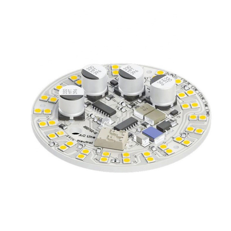
- Product Details
- {{item.text}}
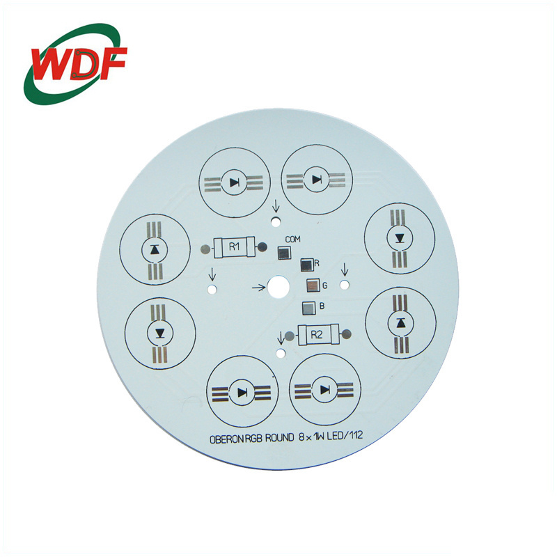
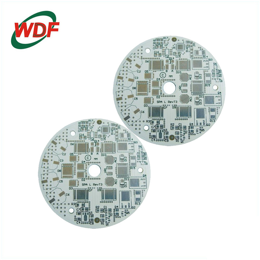
Quick Details
-
Place of Origin:
-
Guangdong, China
-
Brand Name:
-
Wonderful PCB
-
Copper Thickness:
-
0.3 - 6 OZ
-
Min. Hole Size:
-
0.2 mm
-
Min. Line Width:
-
0.1 mm
-
Min. Line Spacing:
-
0.1 mm
-
Surface Finishing:
-
Lead/ Lead-free HASL, ENIG, Silver, OSP
-
Board Size:
-
OEM
-
Item:
-
Wonderful Aluminum PCB Manufacturer
-
Maximum Processing Area:
-
680 x 1000MM
-
Number of Layer:
-
1- 28 Layer
-
Silkscreen color:
-
Black, White, Red, Green
-
MOQ:
-
1 PC
-
Finished Board:
-
Thickness: ≤ 1.0MM, Tolerance:±0.1MM
-
Twisting and Bending:
-
≤ 0.75%, Min: 0.5%
-
Range of TG:
-
130 - 215 ℃
-
Service:
-
One-Stop OEM Service
-
Certificate:
-
ISO9001.ROSH.UL
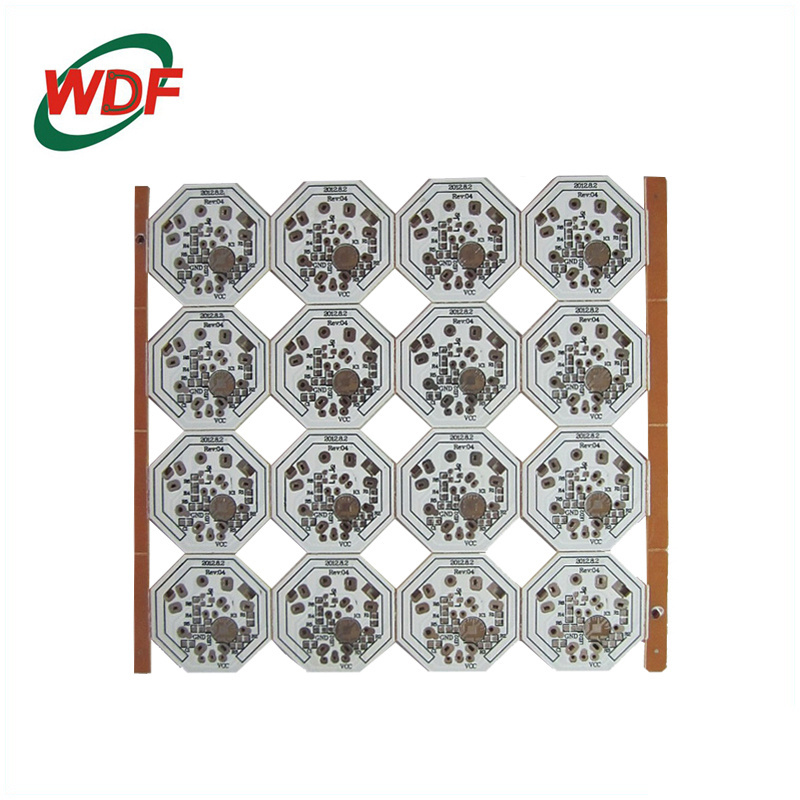
Quick Details
-
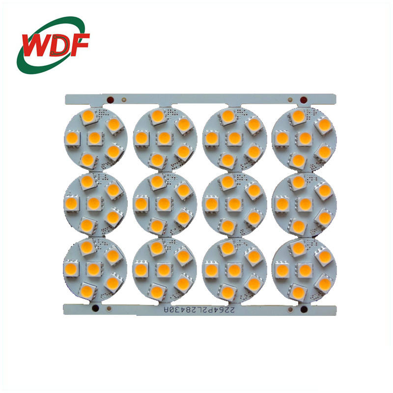
Base Material:
-
Aluminum
-
Board Thickness:
-
0.3mm - 4mm
-
Model Number:
-
Wonderful Aluminum PCB
-
Place of Origin:
-
Guangdong, China
-
Brand Name:
-
Wonderful PCB
-
Copper Thickness:
-
0.3 - 6 OZ
-
Min. Hole Size:
-
0.2 mm
-
Min. Line Width:
-
0.1 mm
-
Min. Line Spacing:
-
0.1 mm
-
Surface Finishing:
-
Lead/ Lead-free HASL, ENIG, Silver, OSP
-
Board Size:
-
OEM
-
Item:
-
Wonderful Aluminum PCB Manufacturer
-
Maximum Processing Area:
-
680 x 1000MM
-
Number of Layer:
-
1- 28 Layer
-
Silkscreen color:
-
Black, White, Red, Green
-
MOQ:
-
1 PC
-
Finished Board:
-
Thickness: ≤ 1.0MM, Tolerance:±0.1MM
-
Twisting and Bending:
-
≤ 0.75%, Min: 0.5%
-
Range of TG:
-
130 - 215 ℃
-
Service:
-
One-Stop OEM Service
-
Certificate:
-
ISO9001.ROSH.UL
If desired, we will source, organise and manage all aspects of the PCB design, so that your product meets all required standards and is fully optimised for easy and cost effective manufacturing.
A well designed circuit board means:
· A reduction in production problems
· Improved quality control
· Reduced costs
· Reduced manufacturing times
We work to supply small and large batches of competitively priced printed circuit boards to our customers.
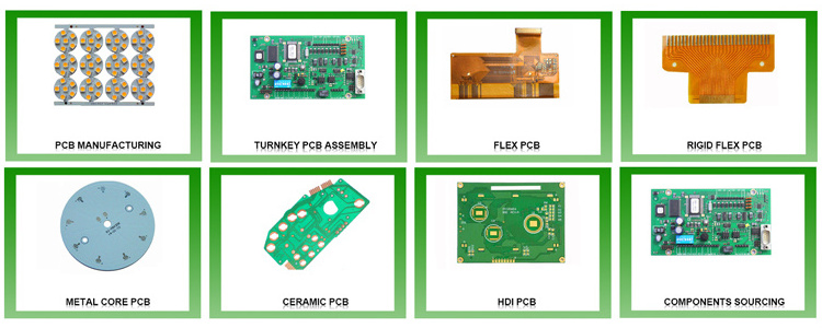
PCB&PCBA Capabilitise
PCB Capability
Number of Layer : 1 - 20 Layer
Maximum Processing Area : 680 × 1000MM
Material : FR1, 22F, CEM-1, CEM-3, FR4,
High TG, Aluminum, Ceramic, Rogers
2 Layer - 0.3MM ( 12 mil )
4 Layer - 0.4MM ( 16mil )
6 Layer - 0.8MM ( 32 mil )
8 Layer - 1.0MM ( 40 mil)
Min Board Thickness :
1
0 Layer - 1.1MM ( 44 mil )
12 Layer - 1.3MM ( 52 mil )
14 Layer - 1.5MM (59 mil )
16 Layer - 1.6MM ( 63 mil )
18Layer - 1.8MM ( 71 mil )
Thickness: ≤ 1.0MM,
Finished Board Tolerance:±0.1MM
Thickness
Tolerance : 1.0MM≤Thickness≤6.5MM
Tolerance ± 10%
Twisting and Bending : ≤ 0.75%, Min: 0.5%
Range of TG : 130 - 215 ℃
Impedance Tolerance : ±10%, Min: ± 5%
Hi-Pot TestMax : 4000V/10MA/60S
HASL, With Lead
HASL Free Lead
Flash Gold
Surface Treatment :
Immersion Gold
Immersion Silver
Immersion Tin
Gold Finger
OSP
PCB Assmbly Capability
Order Quantity : 1pc – 10,000,000+pcs
Build Time : 1 – 5 days, 1 – 2 weeks
or scheduled deliveries
PCB whose width/length is less
than 30mm should be panelized
PCB Spec Requirements :
Max board size: 500×450 mm
Board Type: Rigid PCBs, Flexible
PCBs, Metal core PCBs
Surface mount, Thro-hole
Mixed technology (SMT & Thru-hole)
Assembly Types :
Single or double sided placement
Conformal coating
Shield cover assembly for
EMI
emission
control
Solder Type : Lead-free – RoHS
Full Turnkey
Parts Procurement :
Partial Turnkey
Kitted/Consigned
SMT 01005 or larger
BGA 0.4mm pitch, POP (Package on
Component types : Package), WLCSP 0.35mm pitch
Hard metric connectors,
C
able&wire
SMT Parts
Presentation :
Bulk, Cut tape, Partial reel, Reel
Tube, Tray
Stencils : Laser-cut stainless steel
Free DFM Review, Box Build Assembly
Other Techniques :
100% AOI test and X-ray test for BGA
IC programming, Components cost-down
Function test as custom, Protection tech
It can be a challenge to find the optimal supplier for PCBs – meeting each and all customers’ expectations and requirements on price, quality, lead times, value-added services, and delivery.
Wonderful PCBs
is confidant that we meet each and every expectations for your each PCB.
Production Flow
|
Our advantage
|
|
|
|
|
||||
|
Material Technology
|
Our Production
|
|
|
General Production
|
||||
|
Regular/Special
|
1.Our (TG170)FR4:
high quality materials, excellent heat resistance, won't distort break in high temperature, no foaming, no burning, good performance in electrical charge, impact resistance, humidity-resistance 2.Our FR4 good performance in electrical charge, impact resistance, humidity-resistance 3.Our CEM no-burr 4.Our Rogers Good performance in high frequency 5.Our Aluminum Excellent heat dispersion |
|
|
1.General FR4
High heat work 2.General CEM Expand and deform in damp conditions |
||||
|
Factory
|
We have automatic production line. The automatic production line improves the precision and efficiency of PCB producing,it makes
surface brighter, cleaner and more smooth, and it helps reduce the cost. |
|
|
Artificial production line
|
||||
|
Blind/buried via board, High Density Interconnect(1+1,N+1)
|
Application of HDI technology reducing the thickness and the volume of PCB boards, increasing the density of 3-D wiring design.
|
|
|
Difficult manufacturer, high cost
|
||||
|
Impedance
|
Good performance in reliability and stability of signal sending and receiving
|
|
|
High cost
|
||||
|
Surface Technics
|
1.IMG:smooth surface, good adhesion, no oxidation under long using
2.gold plating(thick gold:1-50U"):good wear-resistance 3.HASL:better price, not easy oxidation, easy to welding, smooth surface 4.HAL: better price, not easy oxidation, easy to welding |
|
|
1.IMG:high price
2.Gold plating(thick gold):high price 3.HAL:surface is not flat, not suitable for BAG packaging |
||||
|
Copper Via/Surface(20-25UM,0.5-60Z)
|
Laser holing: Min 0.1MM, Mechanical holing: Min 0.2MM
|
|
|
Hard to reach 0.1MM
|
||||
|
Multilayer board(4-20 L),BGA(CPU)
|
BGA:high density, high performance, multifunctional, increase thermal reliability, good performance in electroheat property, MIN
width/space: 3/3MIL Multilayer board:strong microporous, high reliability |
|
|
Difficult manufacturer,high cost
|
||||
|
Test
|
To assure quality, avoid wasting after installing and scraping, save cost, save the time of rework
|
|
|
Careless
|
||||
About Us
Contact Us
Hot Searches
