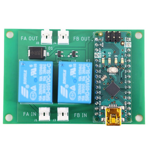
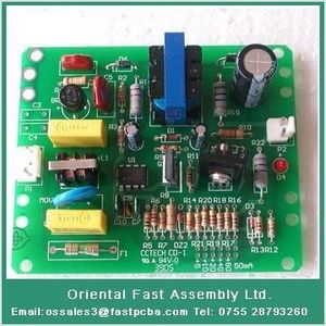
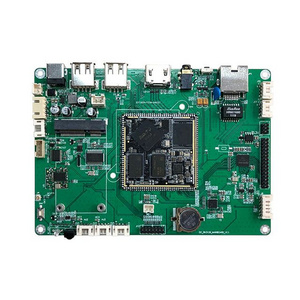
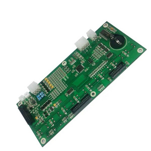
Explore More Products
- Product Details
- {{item.text}}
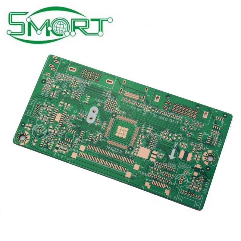
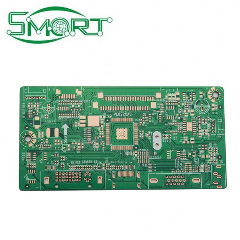
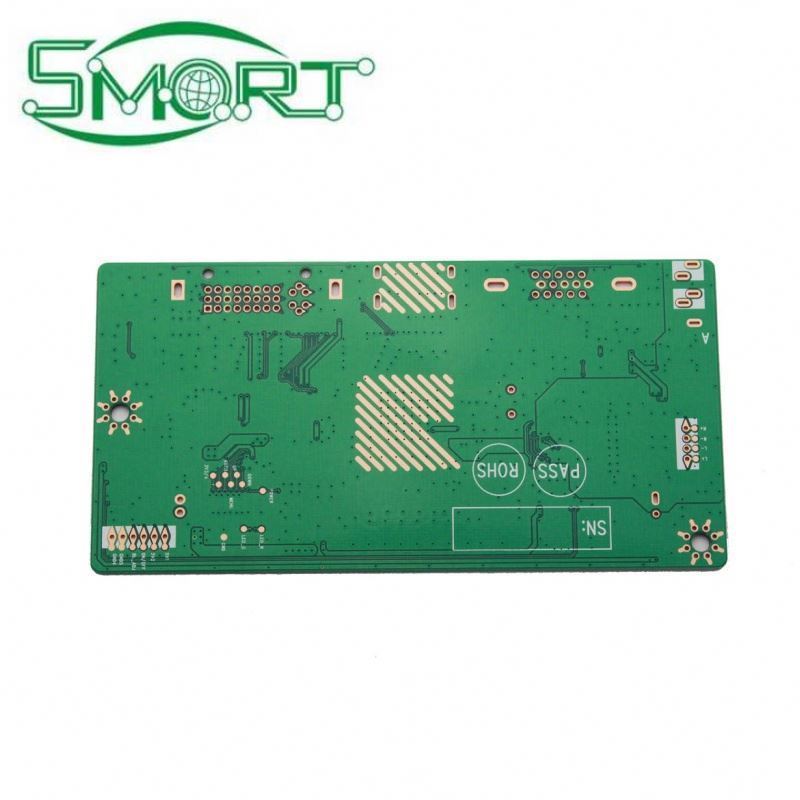
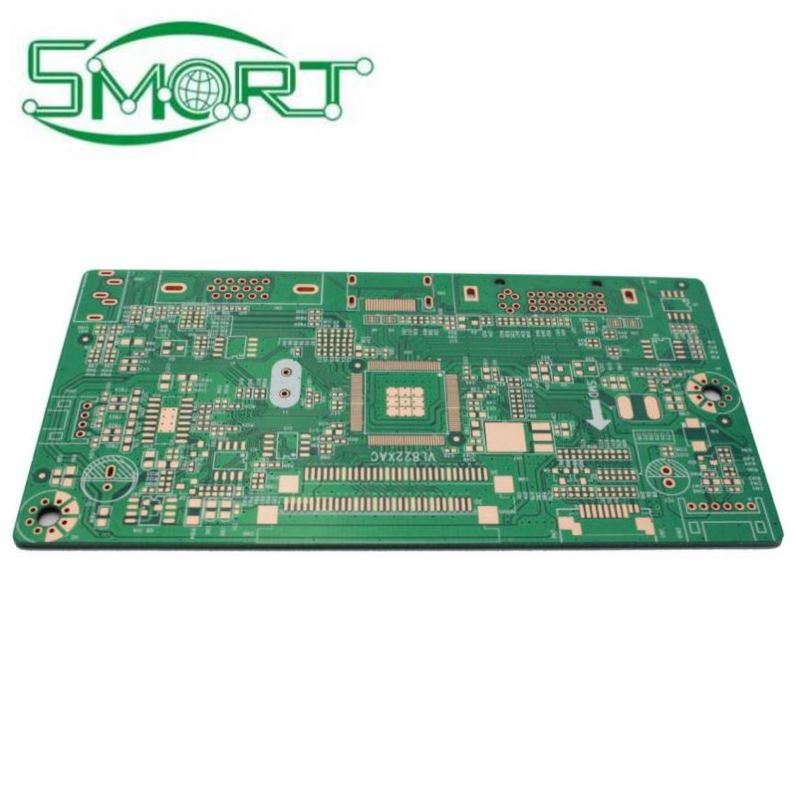
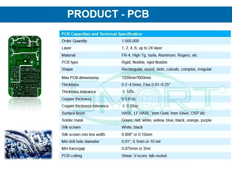
Quick Details
-
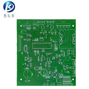
Board Size:
-
custom
-
Model Number:
-
PCB-6 layer
-
Place of Origin:
-
Guangdong, China
-
Brand Name:
-
Smart
-
Copper Thickness:
-
0.5-6.0 oz
-
Min. Hole Size:
-
0.1mm
-
Min. Line Width:
-
0.15mm
-
Min. Line Spacing:
-
0.075mm
-
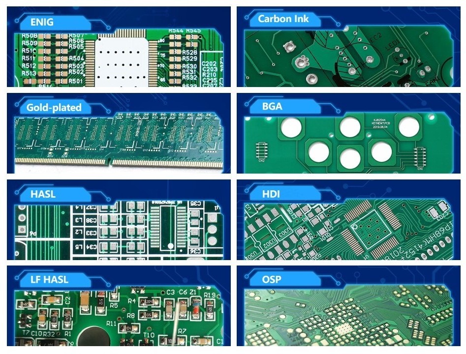
Surface Finishing:
-
ENIG,HASL,Gold-plate, OSP
-
Product name:
-
HASL Multilayer Printed Circuit Board
-
pcb:
-
single side pcb ,double side pcb,multilayer pcb Packaging & Delivery
-
Certification:
-
ROHS, ISO9001:2000
-
Shape:
-
Rectangular, round, slots, cutouts, complex, irregular
-
Solder mask color:
-
Green, red, white, yellow, blue, black, orange, purple
-
Silk screen:
-
White, black
-
Silk scre en min line width:
-
0.006" or 0.15mm
-
Min drill hole diameter:
-
0.01", 0.1mm or 10 mil
-
Min trace / gap:
-
0.075mm or 3mil
-
PCB cutting:
-
Shear, V-score, tab-routed
Quick Details
-
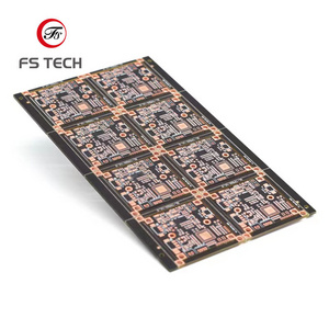
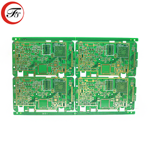
Number of Layers:
-
2/4/6/8/12/14 or custom
-
Base Material:
-
FR4, TG, CEM-1, Aluminium
-
Board Thickness:
-
0.2-4.0mm
-
Board Size:
-
custom
-
Model Number:
-
PCB-6 layer
-
Place of Origin:
-
Guangdong, China
-
Brand Name:
-
Smart
-
Copper Thickness:
-
0.5-6.0 oz
-
Min. Hole Size:
-
0.1mm
-
Min. Line Width:
-
0.15mm
-
Min. Line Spacing:
-
0.075mm
-
Surface Finishing:
-
ENIG,HASL,Gold-plate, OSP
-
Product name:
-
HASL Multilayer Printed Circuit Board
-
pcb:
-
single side pcb ,double side pcb,multilayer pcb Packaging & Delivery
-
Certification:
-
ROHS, ISO9001:2000
-
Shape:
-
Rectangular, round, slots, cutouts, complex, irregular
-
Solder mask color:
-
Green, red, white, yellow, blue, black, orange, purple
-
Silk screen:
-
White, black
-
Silk scre en min line width:
-
0.006" or 0.15mm
-
Min drill hole diameter:
-
0.01", 0.1mm or 10 mil
-
Min trace / gap:
-
0.075mm or 3mil
-
PCB cutting:
-
Shear, V-score, tab-routed


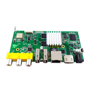
CUSTOM PCB&PCBA,Please send us gerber file and bom list.
|
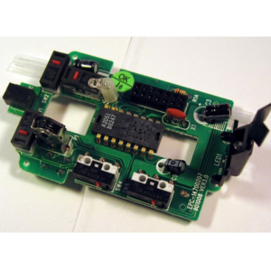
PCBA
|
PCB+components sourcing+assembly+package
|
|
Assembly details
|
SMT and Thru-hole, ISO SMT and DIP lines
|
|
Lead Time
|
Prototype : 15 work days. Mass order : 20~25 work days
|
|
Testing on products
|
Testing jig/mold , X-ray Inspection, AOI Test, Functional test
|
|
Quantity
|
Min quantity : 1pcs. Prototype, small order, mass order, all OK
|
|
Files needed
|
PCB : Gerber files(CAM, PCB, PCBDOC)
Components : Bill of Materials(BOM list) Assembly : Pick-N-Place file |
|
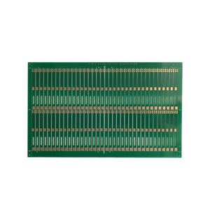
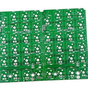
PCB Panel Size
|
Min size : 0.25*0.25 inches(6*6mm)
Max size : 1200*600mm |
|
Components details
|
Passive Down to 0201 size
BGA and VFBGA Leadless Chip Carriers/CSP Double-sided SMT Assembly Fine Pitch to 0.8mils BGA Repair and Reball Part Removal and Replacement |
|
Component package
|
Cut Tape, Tube, Reels, Loose Parts
|
|
PCB+ assembly process
|
Drilling-----Exposure-----Plating-----Etaching & Stripping-----Punching-----Electrical Testing-----SMT-----Wave Soldering-----Assembling-----ICT-----Function Testing-----Temperature & Humidity Testing
|
Hot Searches
