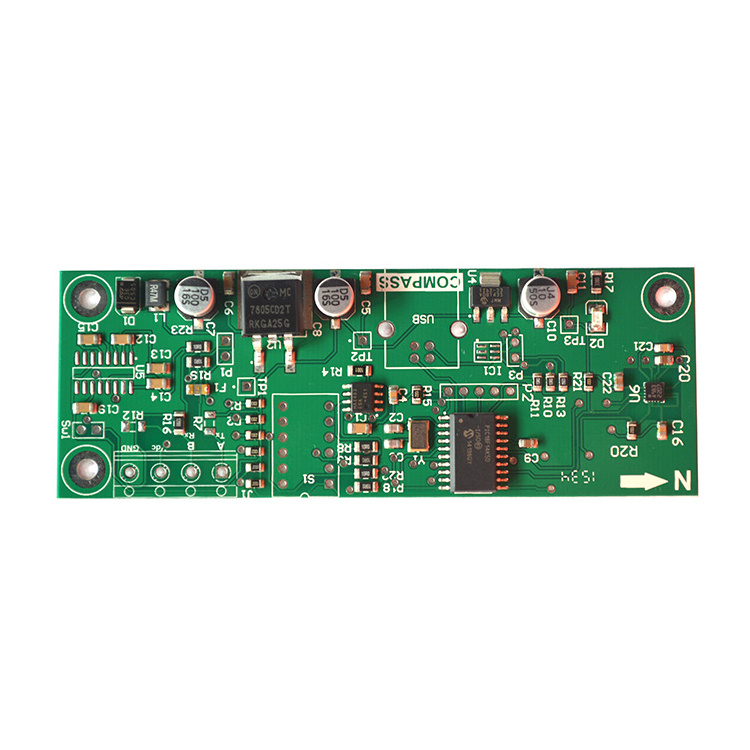
- Product Details
- {{item.text}}
Quick Details
-
Board Size:
-
200*200MM
-
Model Number:
-
PCBA - 20.06
-
Place of Origin:
-
Guangdong, China
-
Brand Name:
-
MOKO - PCB
-
Copper Thickness:
-
1OZ
-
Min. Hole Size:
-
0.2MM
-
Min. Line Width:
-
0.1MM
-
Min. Line Spacing:
-
0.1MM
-
Surface Finishing:
-
HASL Lead free; ENIG
-
Max Panel size:
-
500*500mm
-
Service type:
-
PCB,Turnkey PCBA,PCB clone, PCBA enclosure assembly
-
High PCB technique:
-
Blind &buried via+Impedance control
-
PCB QC:
-
Flying Probe Test,E-test
-
PCBA QC:
-
X-ray,AOI Test, FCT Equipment
-
PCBA Prototype:
-
Support sample order
-
Lead time:
-
Prototypes:15 days,Mass production:20 days
-
Certification:
-
ROHS,ISO14001:2004,ISO9001:2000
Quick Details
-
Number of Layers:
-
4-layer
-
Base Material:
-
FR4
-
Board Thickness:
-
1.6MM
-
Board Size:
-
200*200MM
-
Model Number:
-
PCBA - 20.06
-
Place of Origin:
-
Guangdong, China
-
Brand Name:
-
MOKO - PCB
-
Copper Thickness:
-
1OZ
-
Min. Hole Size:
-
0.2MM
-
Min. Line Width:
-
0.1MM
-
Min. Line Spacing:
-
0.1MM
-
Surface Finishing:
-
HASL Lead free; ENIG
-
Max Panel size:
-
500*500mm
-
Service type:
-
PCB,Turnkey PCBA,PCB clone, PCBA enclosure assembly
-
High PCB technique:
-
Blind &buried via+Impedance control
-
PCB QC:
-
Flying Probe Test,E-test
-
PCBA QC:
-
X-ray,AOI Test, FCT Equipment
-
PCBA Prototype:
-
Support sample order
-
Lead time:
-
Prototypes:15 days,Mass production:20 days
-
Certification:
-
ROHS,ISO14001:2004,ISO9001:2000
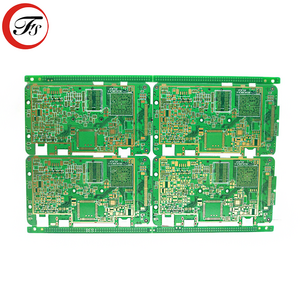
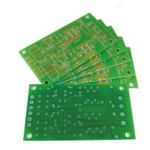
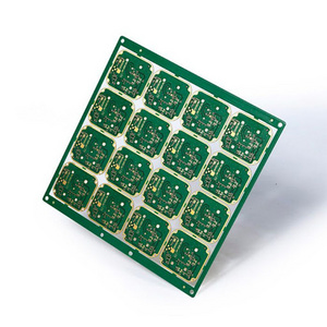
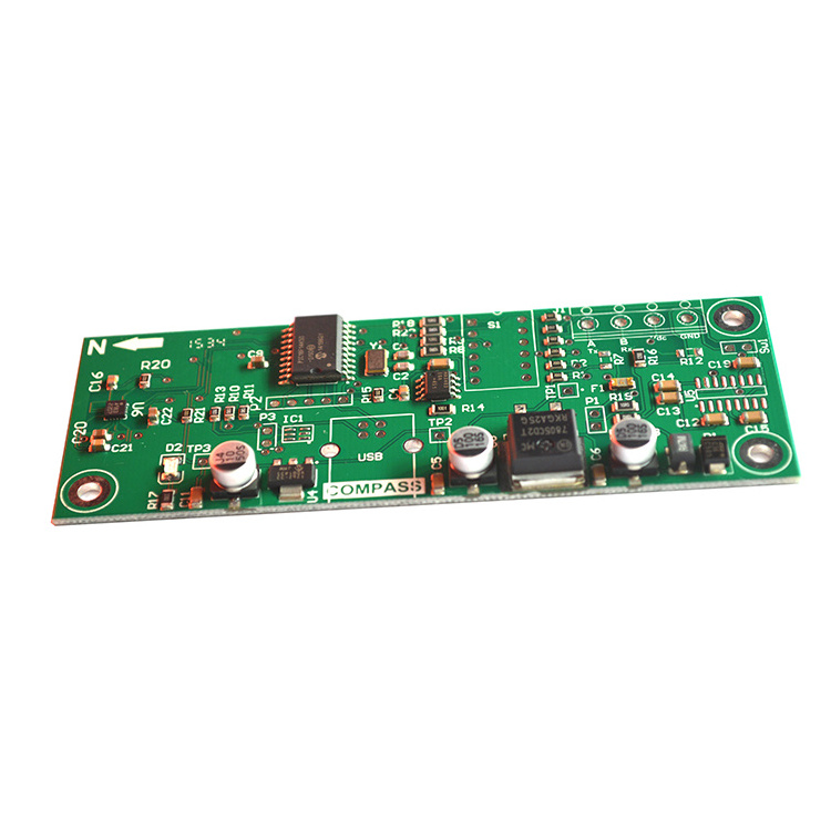
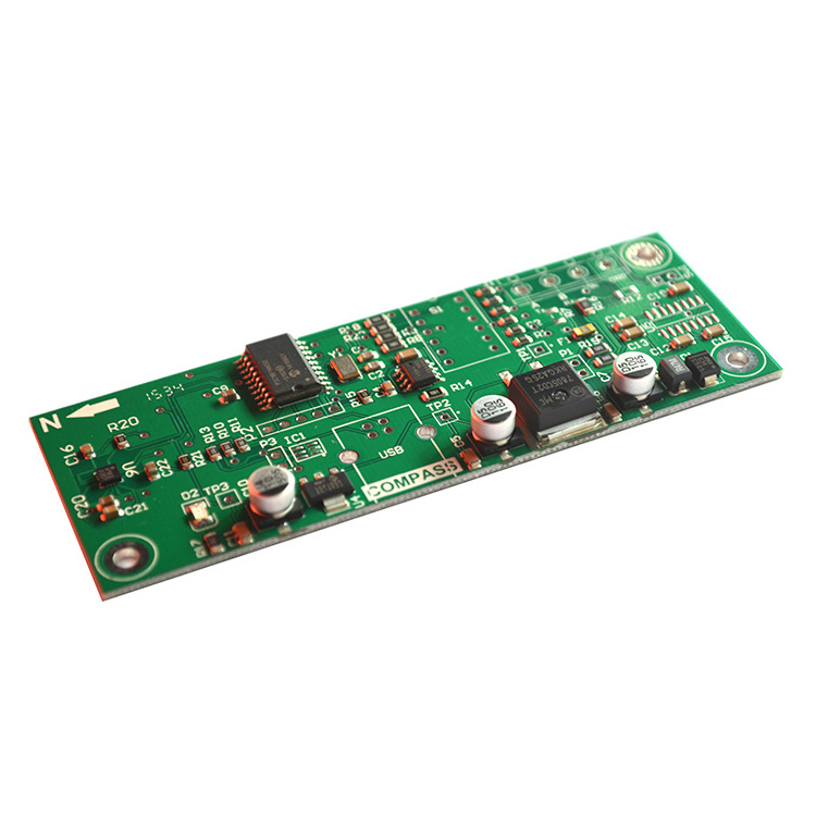
Electronics prototype custom FR4 PCB manufacturer printed circuit board fabrication
PCB Technical Specification
| Number of Layer | 1,2,4 or 6,upto 18 layer |
| Order Quantity | 1 to 50,000 |
| Board Shape | Retangular,round,slots,cutouts,complex,irregular |
| Board Type | Rigid, Flexible, Rigid-flexible |
| Board Material | FR-4 glass epoxy, FR-4 high Tg, Rohs compliant,Aluminum,Rogers,etc. |
| Board Cutting | Shear,V-score,Tab-routed |
| Board Thickness | 0.2-4.0mm, Flex 0.01-0.25mm |
| Copper Weight | 1.0, 1.5, 2.0 oz |
| Solder Mask | Double-sided green LPI,Also support Red,White,Yellow,Blue,Black |
| Silk Screen | Double-sided or single-sided in white,yellow,black,or negative |
| Silk Screen Min Line Width | 0.006'' or 0.15mm |
| Max Board Dimensions | 20 inch*20inch or 500mm*500mm |
| Min Trace/Gap | 0.10mm, or 4mils |
| Min Drill Hole Diameter | 0.01'',0.25mm, or 10mils |
| Surface Finish | HASL,Nickle,Immersion Gold,Immersion Tin,Immersion Silver,OSP,etc. |
| Board Thickness Tolerance | ±10% |
| Copper Weight Tolerance | ± 0.25 oz |
| Minimal Slot Width | 0.12'', 3.0mm, or 120mils |
| V-Score Depth | 20-25% of board thickness |
| Design File Formate | Gerber RS-274,274D,Eagle and AutoCAD's DXF,DWG |
PCBA Capabilities
| Quantity | Prototype&Low Volume PCB Assembly,from 1 Board to 250,is specialty,or up to 1000 |
| Type of Assembly | SMT,Thru-hole |
| Solder Type | Water Soluble Solder Paste,Leaded and Lead-Free |
| Components |
Passive Down to 0201 size BGA and VFBGA Leadless Chip Carriers/CSP Double-sided SMT Assembly Fine Pitch to 0.8mils BGA Repair and Reball Part Removal and Replacement |
| Bare Board Size |
Smallest:0.25*0.25 inches Largest:20*20 inches |
| File Formate |
Bill of Materials Gerber files Pick-N-Place file |
| Types of Service | Turn-key,partial turn-key or consignment |
| Component packaging | Cut Tape,Tube,Reels,Loose Parts |
| Turn Time | Same day service to 15 days service |
| Testing | Flying Probe Test,X-ray Inspection AOI Test |
| PCB assembly process |
Drilling-----Exposure-----Plating-----Etaching & Stripping-----Punching-----Electrical Testing-----SMT-----Wave Soldering-----Assembling-----ICT-----Function Testing-----Temperature & Humidity Testing |
Technical requirement for pcb&pcb assembly:
1. Professional Surface-mounting and Through-hole soldering Technology
2. Various sizes like 1206,0805,0603 components SMT technology
3.ICT(In Circuit Test),FCT(Functional Circuit Test) technology.
4.PCB Assembly With UL,CE,FCC,Rohs Approval
5.Nitrogen gas reflow soldering technology for SMT.
6.High Standard SMT&Solder Assembly Line
7. High density interconnected board placement technology capacity.
Quotation requirement for pcb&pcb assembly:
1. PCB gerber file
2. BOM list for PCBA
3. Sample of PCB and PCBA
4.Test method for PCBA
Lead time:
|
PCB |
Single/double side |
4 layer |
6 layer |
Above 8 layer |
HDI |
|
Sample lead time(Normal) |
5-6 |
6-7 |
7-8 |
10-12 |
15-20 |
|
Sample lead time(Fastest) |
48-72 hours |
5 |
6 |
6-7 |
12 |
|
Mass production lead time(First batch) |
7-9 |
10-12 |
13-15 |
16 |
20 |
|
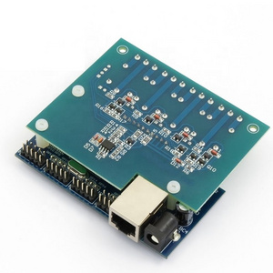
PCB Assembly |
PCB Fab+Components Sourcing+PCBA= 20 days |
||||
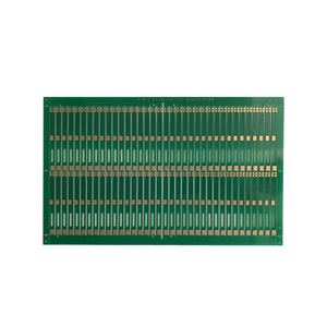
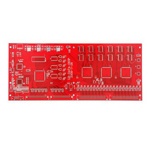
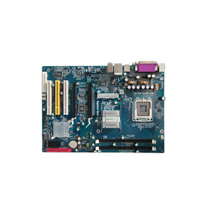
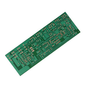
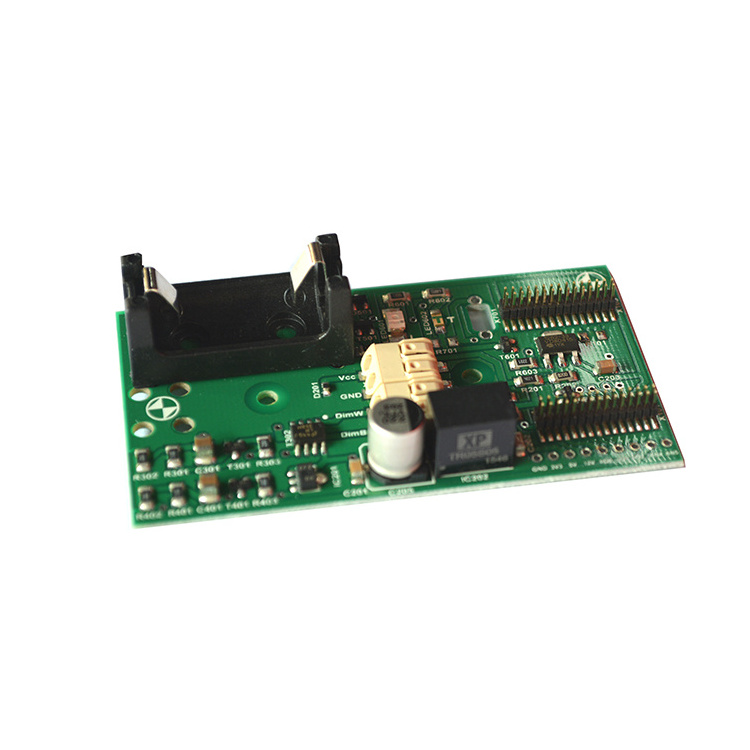
relating product show

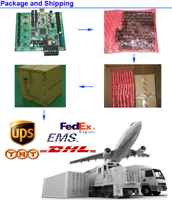
1.PCB
2.Component service
3.PCB Assembly
4.PCBA testing
5. PCB Assembly with Enclosure
Our Advantage:
PCB quoted online
Original ICs and compoennts from stock
High quality PCBA and competitive price
100% PCBA function testing
Warranty: 2 Years
Shortly lead time: PCB :4-9 days,PCBA:20-25days
Certificate:UL,ROHS,CE,ISO9001,ISO14001
PCBA OEM service with more than 10 years experience
PCB Sample Cost:
Notes:The Following Cost for the Special Samples Cost, the cost only for pcb cost, the film cost and tool cost will be based on the pcb file you provided.quantity below 10pcs. (Unit:mm)
| 1-2 Layer | 4 LAYER | 6 Layer | 8 Layer |
| Below 3*3 5.3USD | Below 5*5 67.0USD | Below 5*5 167.0USD | Below 5*5 317.0 |
| Below 5*5 8.8USD | Below 10*10 84.0USD | Below 10*10 184USD | Below 10*10 350.2USD |
| Below 10*10 $17.1 |
Batch Quantity Cost:
Notes: The Following Cost don't include the Engineer Cost.
| PCB Thickness(mm) | 2 Layer(/M^2) | 4 Layer(/M^2) | 6 Layer(/ M^2) | 8 Layer (/M^2) |
| 0.4~0.8 | 65.3USD | 133.3USD | ||
| 1.0~1.2 | 65.5USD | 138.3USD | 208.5USD | 283.5USD |
| 1.6 | 67.0USD | 142.0USD | 217.0USD | 300.2USD |
| 2.0 | 70.2USD | 150.3USD | 300.0USD | 333.5USD |
| 2.4 | 100.2USD | 158.5USD | 367.0USD | 366.8USD |
| 3.0 | 108.2USD | 200.2USD | 400.3USD | 433.5USD |