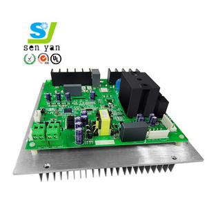
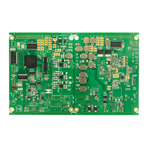
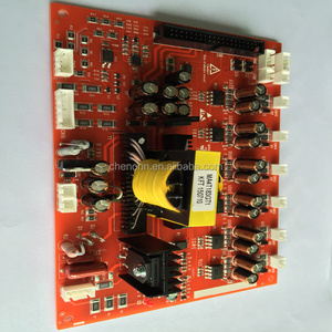
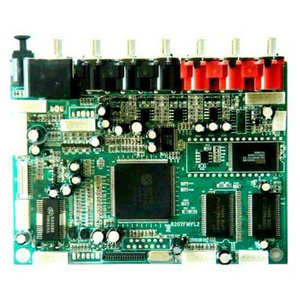
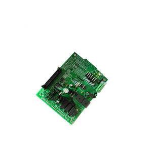
- Product Details
- {{item.text}}
Quick Details
-
Place of Origin:
-
Guangdong, China
-
Brand Name:
-
WDF
-
Copper Thickness:
-
1oz
-
Min. Hole Size:
-
0.5mm
-
Min. Line Width:
-
0.12mm
-
Min. Line Spacing:
-
0.15mm
-
Surface Finishing:
-
HASL lead free
-
Board Size:
-
OEM
-
Product name:
-
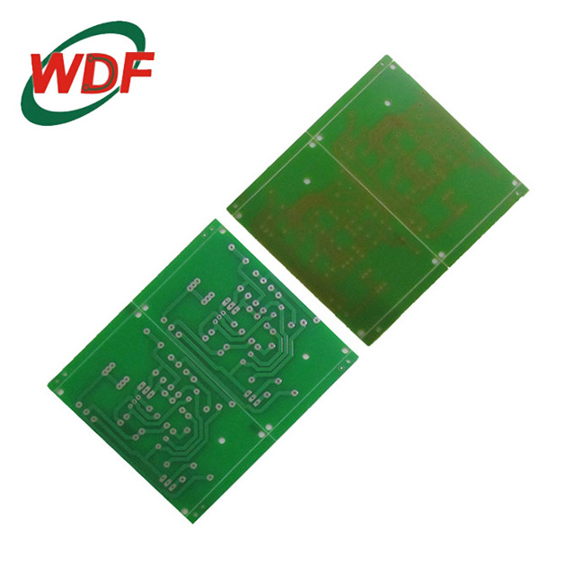
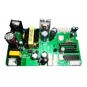
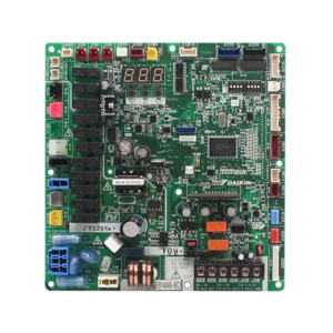
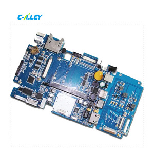
Double Layer Pcb Assembly Manufacturer
-
Max Panel Size:
-
1000mm*600mm
-
Solder Mask:
-
Green, Red, Blue, Yellow, etc.
-
Silk Screen:
-
White, Black, Yellow, Red, Blue,etc
-
Certification:
-
UL, SGS, RoHS, ISO14001, ISO9001-2000
-
Profiling puching:
-
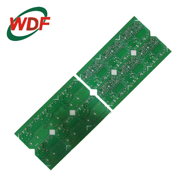
V-cut, rounting, beveling
-
Test:
-
X-ray, AOI Test, functional test
-
Specialized in:
-
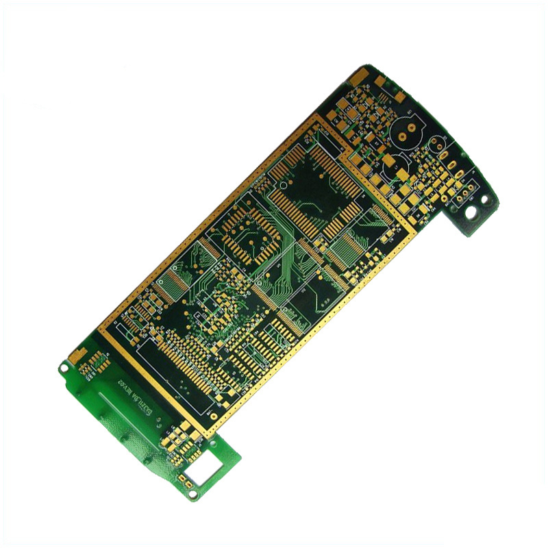
High-precision, high-density, double-sided PCB, multilayer PCB
-
Application:
-
electronic product,Smart Home
-
Delivery Time:
-
7 days
Quick Details
-
Base Material:
-
FR4
-
Board Thickness:
-
1.6mm
-
Model Number:
-
WDF01
-
Place of Origin:
-
Guangdong, China
-
Brand Name:
-
WDF
-
Copper Thickness:
-
1oz
-
Min. Hole Size:
-
0.5mm
-
Min. Line Width:
-
0.12mm
-
Min. Line Spacing:
-
0.15mm
-
Surface Finishing:
-
HASL lead free
-
Board Size:
-
OEM
-
Product name:
-
Double Layer Pcb Assembly Manufacturer
-
Max Panel Size:
-
1000mm*600mm
-
Solder Mask:
-
Green, Red, Blue, Yellow, etc.
-
Silk Screen:
-
White, Black, Yellow, Red, Blue,etc
-
Certification:
-
UL, SGS, RoHS, ISO14001, ISO9001-2000
-
Profiling puching:
-
V-cut, rounting, beveling
-
Test:
-
X-ray, AOI Test, functional test
-
Specialized in:
-
High-precision, high-density, double-sided PCB, multilayer PCB
-
Application:
-
electronic product,Smart Home
-
Delivery Time:
-
7 days

If desired, we will source, organise and manage all aspects of the PCB design, so that your product meets all required standards and is fully optimised for easy and cost effective manufacturing.
A well designed circuit board means:
· A reduction in production problems
· Improved quality control
· Reduced costs
· Reduced manufacturing times
We work to supply small and large batches of competitively priced printed circuit boards to our customers.
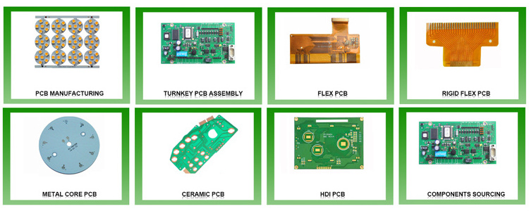
PCB&PCBA Capabilitise

PCB Capability
Number of Layer : 1 - 20 Layer
Maximum Processing Area : 680 × 1000MM
Material : FR1, 22F, CEM-1, CEM-3, FR4,
High TG, Aluminum, Ceramic, Rogers
2 Layer - 0.3MM ( 12 mil )
4 Layer - 0.4MM ( 16mil )
6 Layer - 0.8MM ( 32 mil )
8 Layer - 1.0MM ( 40 mil)
Min Board Thickness :
1
0 Layer - 1.1MM ( 44 mil )
12 Layer - 1.3MM ( 52 mil )
14 Layer - 1.5MM (59 mil )
16 Layer - 1.6MM ( 63 mil )
18Layer - 1.8MM ( 71 mil )
Thickness: ≤ 1.0MM,
Finished Board Tolerance:±0.1MM
Thickness
Tolerance : 1.0MM≤Thickness≤6.5MM
Tolerance ± 10%
Twisting and Bending : ≤ 0.75%, Min: 0.5%
Range of TG : 130 - 215 ℃
Impedance Tolerance : ±10%, Min: ± 5%
Hi-Pot TestMax : 4000V/10MA/60S
HASL, With Lead
HASL Free Lead
Flash Gold
Surface Treatment :
Immersion Gold
Immersion Silver
Immersion Tin
Gold Finger
OSP
PCB Assmbly Capability
Order Quantity : 1pc – 10,000,000+pcs
Build Time : 1 – 5 days, 1 – 2 weeks
or scheduled deliveries
PCB whose width/length is less
than 30mm should be panelized
PCB Spec Requirements :
Max board size: 500×450 mm
Board Type: Rigid PCBs, Flexible
PCBs, Metal core PCBs
Surface mount, Thro-hole
Mixed technology (SMT & Thru-hole)
Assembly Types :
Single or double sided placement
Conformal coating
Shield cover assembly for
EMI
emission
control
Solder Type : Lead-free – RoHS
Full Turnkey
Parts Procurement :
Partial Turnkey
Kitted/Consigned
SMT 01005 or larger
BGA 0.4mm pitch, POP (Package on
Component types : Package), WLCSP 0.35mm pitch
Hard metric connectors,
C
able&wire
SMT Parts
Presentation :
Bulk, Cut tape, Partial reel, Reel
Tube, Tray
Stencils : Laser-cut stainless steel
Free DFM Review, Box Build Assembly
Other Techniques :
100% AOI test and X-ray test for BGA
IC programming, Components cost-down
Function test as custom, Protection tech
It can be a challenge to find the optimal supplier for PCBs – meeting each and all customers’ expectations and requirements on price, quality, lead times, value-added services, and delivery.
Wonderful PCBs
is confidant that we meet each and every expectations for your each PCB.
Production Flow
|
Our advantage
|
|
|
|
|
||||
|
Material Technology
|
Our Production
|
|
|
General Production
|
||||
|
Regular/Special
|
1.Our (TG170)FR4:
high quality materials, excellent heat resistance, won't distort break in high temperature, no foaming, no burning, good performance in electrical charge, impact resistance, humidity-resistance 2.Our FR4 good performance in electrical charge, impact resistance, humidity-resistance 3.Our CEM no-burr 4.Our Rogers Good performance in high frequency 5.Our Aluminum Excellent heat dispersion |
|
|
1.General FR4
High heat work 2.General CEM Expand and deform in damp conditions |
||||
|
Factory
|
We have automatic production line. The automatic production line improves the precision and efficiency of PCB producing,it makes
surface brighter, cleaner and more smooth, and it helps reduce the cost. |
|
|
Artificial production line
|
||||
|
Blind/buried via board, High Density Interconnect(1+1,N+1)
|
Application of HDI technology reducing the thickness and the volume of PCB boards, increasing the density of 3-D wiring design.
|
|
|
Difficult manufacturer, high cost
|
||||
|
Impedance
|
Good performance in reliability and stability of signal sending and receiving
|
|
|
High cost
|
||||
|
Surface Technics
|
1.IMG:smooth surface, good adhesion, no oxidation under long using
2.gold plating(thick gold:1-50U"):good wear-resistance 3.HASL:better price, not easy oxidation, easy to welding, smooth surface 4.HAL: better price, not easy oxidation, easy to welding |
|
|
1.IMG:high price
2.Gold plating(thick gold):high price 3.HAL:surface is not flat, not suitable for BAG packaging |
||||
|
Copper Via/Surface(20-25UM,0.5-60Z)
|
Laser holing: Min 0.1MM, Mechanical holing: Min 0.2MM
|
|
|
Hard to reach 0.1MM
|
||||
|
Multilayer board(4-20 L),BGA(CPU)
|
BGA:high density, high performance, multifunctional, increase thermal reliability, good performance in electroheat property, MIN
width/space: 3/3MIL Multilayer board:strong microporous, high reliability |
|
|
Difficult manufacturer,high cost
|
||||
|
Test
|
To assure quality, avoid wasting after installing and scraping, save cost, save the time of rework
|
|
|
Careless
|
||||
About Us
Contact Us
Hot Searches
