- Product Details
- {{item.text}}
Quick Details
-
Place of Origin:
-
Guangdong, China
-
Copper Thickness:
-
1 Oz
-
Min. Hole Size:
-
0.8mm
-
Min. Line Width:
-
0.32mm
-
Min. Line Spacing:
-
0.3mm
-
Surface Finishing:
-
HASL Lead Free
-
Board Size:
-
Customized
-
Solder mask:
-
White
-
Application:
-
LED Lighting
Quick Details
-
Base Material:
-
Aluminum Base
-
Board Thickness:
-
1.6mm
-
Model Number:
-
MPCB 001
-
Place of Origin:
-
Guangdong, China
-
Copper Thickness:
-
1 Oz
-
Min. Hole Size:
-
0.8mm
-
Min. Line Width:
-
0.32mm
-
Min. Line Spacing:
-
0.3mm
-
Surface Finishing:
-
HASL Lead Free
-
Board Size:
-
Customized
-
Solder mask:
-
White
-
Application:
-
LED Lighting
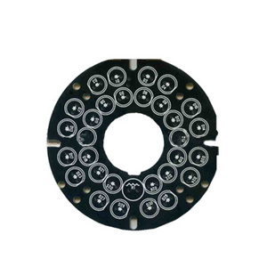
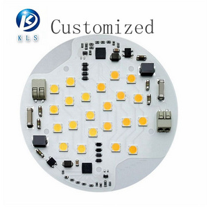
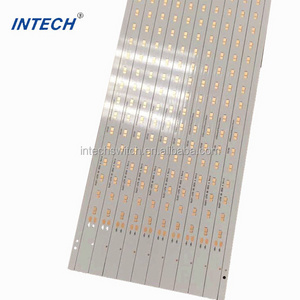
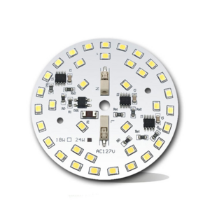
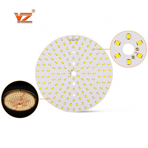
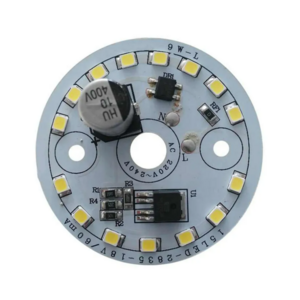
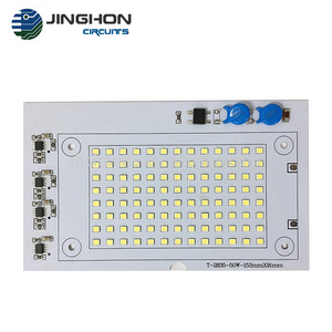
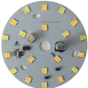
Mass Production Bended Aluminum Base Copper base Mcpcb LED PCB for LED lighting
Large Quantity Copper base Aluminum Base PCB for 5730 Smd Led Specifications.
Copper base Aluminum Base PCB is made by three layers, circuit layer, dielectric layer and metal base layer. Circuit Layer is made of copper which is 0.5-10 oz. The dielectric layer owns key technologies of metal base lamination which will lead to different characteristics of the material. Its thickness is between 50 to 200 um. Metal base layer can be made of aluminum or copper.
Comparing to FR-4 lamination boards, Copper base Aluminum Base PCB has the advantages of :
1, H igh thermal conductivity
2, Excellent thermal diffusivity
3, Good electrical insulation
4, Products can be of smaller size by removing radiator parts .
5, High withstand voltage of metal base material is up to 4500V.
So Copper base Aluminum Base PCB is widely applied to high power products, i.e LED, power supply, high voltage or currency products.
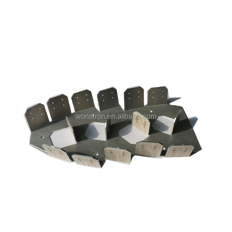
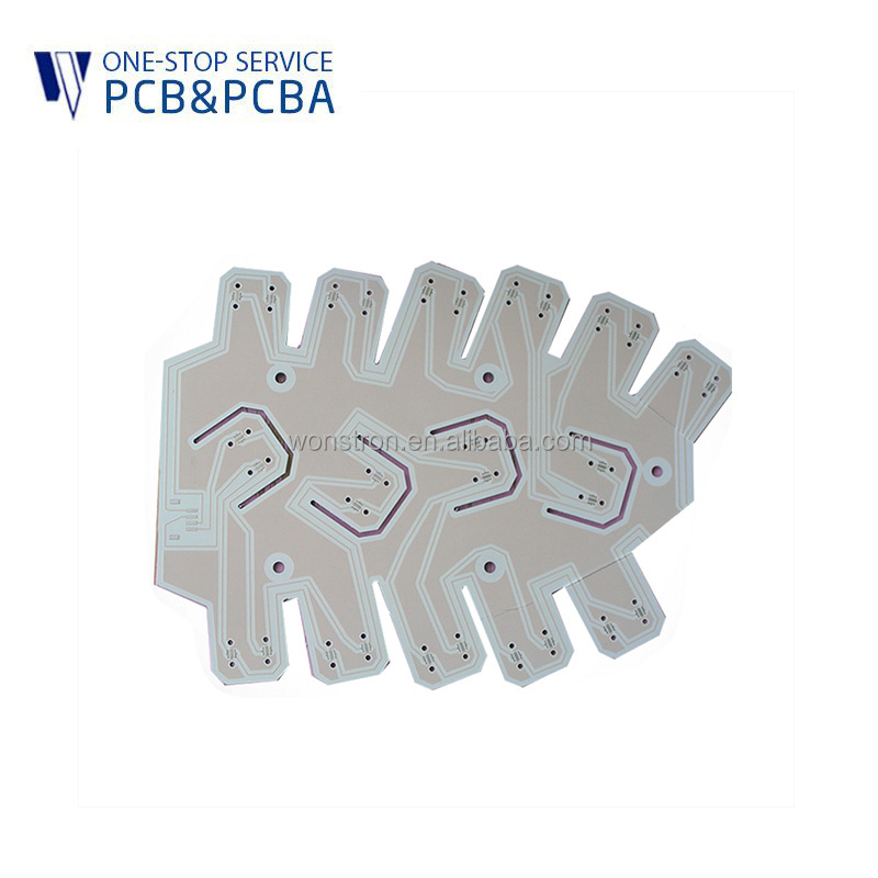
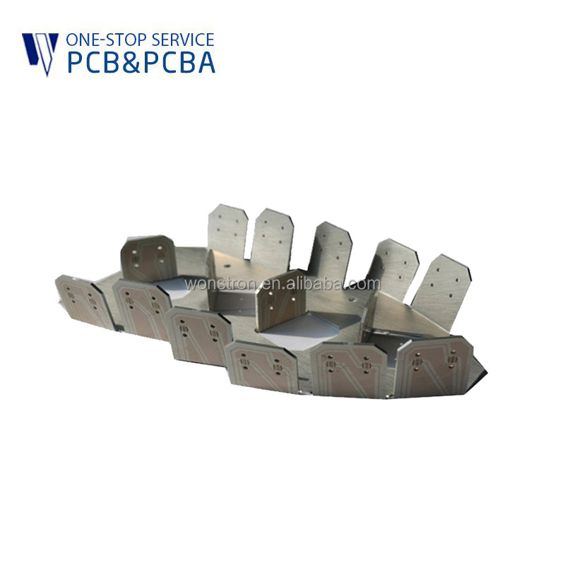
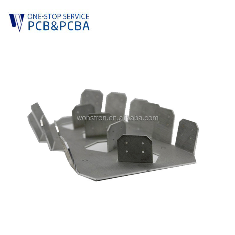
This is a special LED design from a famous LED brand. The Aluminum Base PCB is bended to different angles to achieve well-distributed light. By this way the aluminum base is routing to 2/3 depth and the copper layer would be with extremely flexible. It is a challenge to both machines and material.
Our Manufacture Capacity
|
Item |
Mass Production |
Sample |
|
Main Material |
Bergquist,Laird,SANYO |
|
|
Metal Type |
Aluminum base,Copper base |
|
|
Min Line Width/Space |
0.1mm/ 0.1mm |
0.075 mm / 0.075 mm |
|
Min Drilling Diameter |
φ 0 .55mm |
φ 0.55mm |
|
Max. Copper Thickness |
4 Oz |
6 Oz |
|
Thermal conductivity |
1W/mK , 2W/mK |
|
|
Dielectric Thickness |
50-200um |
|
|
Layers |
1-4 Layer |
|
|
Max Drilling Aspect Ratio |
8:1 |
|
|
Max Panel Size |
703mm × 550mm |
|
|
Finished Board Thickness |
0.4-3.2mm |
|
|
Production Per Month |
15,000 m ² |
|
Production Lead Time
|
Item |
Sample |
Mass Production |
|
Single-Layer |
2-4 days |
3-5 days |
|
Double-sided |
2-5 days |
5-15 days |
|
Multi-Layer Boards |
5-10 days |
8-20 days |
|
*Special material ordered l ead time is not included. |
||