Explore More Products
- Product Details
- {{item.text}}
Quick Details
-
Supplier Type:
-
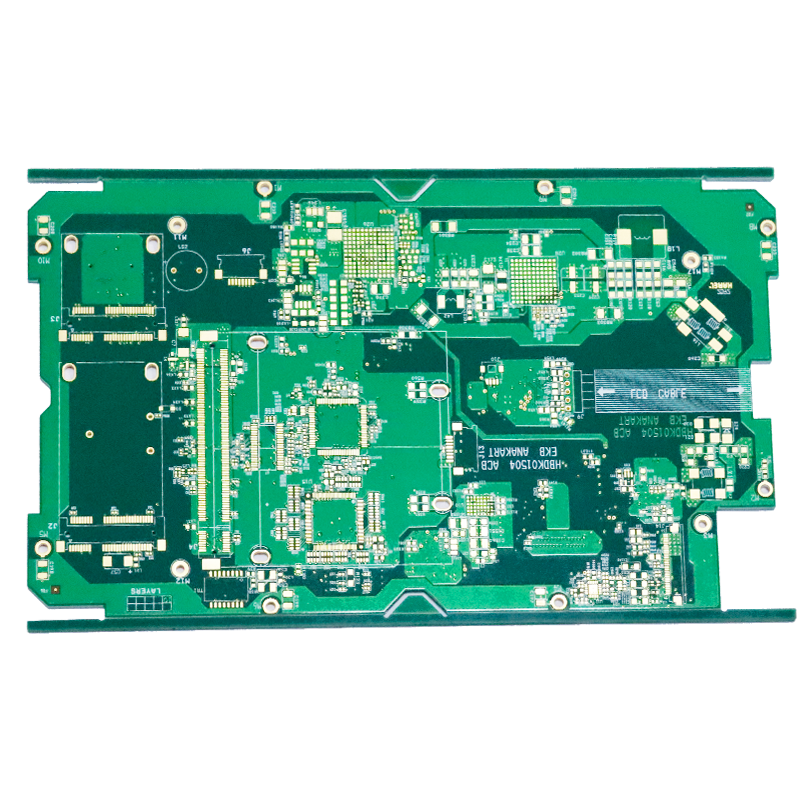
Customized PCB
-
Max layer:
-
16 layers
-
Min. hole size:
-
10mil
-
Min. line width/space:
-
0.1mm
-
Hole position tolerance:
-
+/-0.076mm
-
Routing outline tolerance:
-
+/-0.13mm
-
Punching outline tolerance:
-
+/-0.05mm
-
Production capability:
-
40,000 s.q.m/month
-
Surface finished:
-
Lead free HASL, immersion gold (ENIG), immersion silver, immersion Tin
-
Solder mask:
-
Green. Red. Blue. White. Black
Quick Details
-
Model Number:
-
2sc5200 2sa1943 transistor
-
Place of Origin:
-
Guangdong, China
-
Brand Name:
-
finest PCB
-
Supplier Type:
-
Customized PCB
-
Max layer:
-
16 layers
-
Min. hole size:
-
10mil
-
Min. line width/space:
-
0.1mm
-
Hole position tolerance:
-
+/-0.076mm
-
Routing outline tolerance:
-
+/-0.13mm
-
Punching outline tolerance:
-
+/-0.05mm
-
Production capability:
-
40,000 s.q.m/month
-
Surface finished:
-
Lead free HASL, immersion gold (ENIG), immersion silver, immersion Tin
-
Solder mask:
-
Green. Red. Blue. White. Black
Our Services
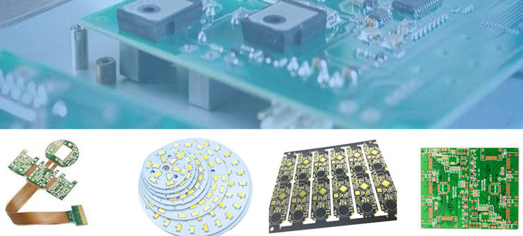
Finest PCB Assembly is a 18 years one-stop solution provide:
*PCB manufacturing
*Components sourcing
*PCB assembly
*Firmware programming
*PCBA functional test
*Plastic/Metal case assembly
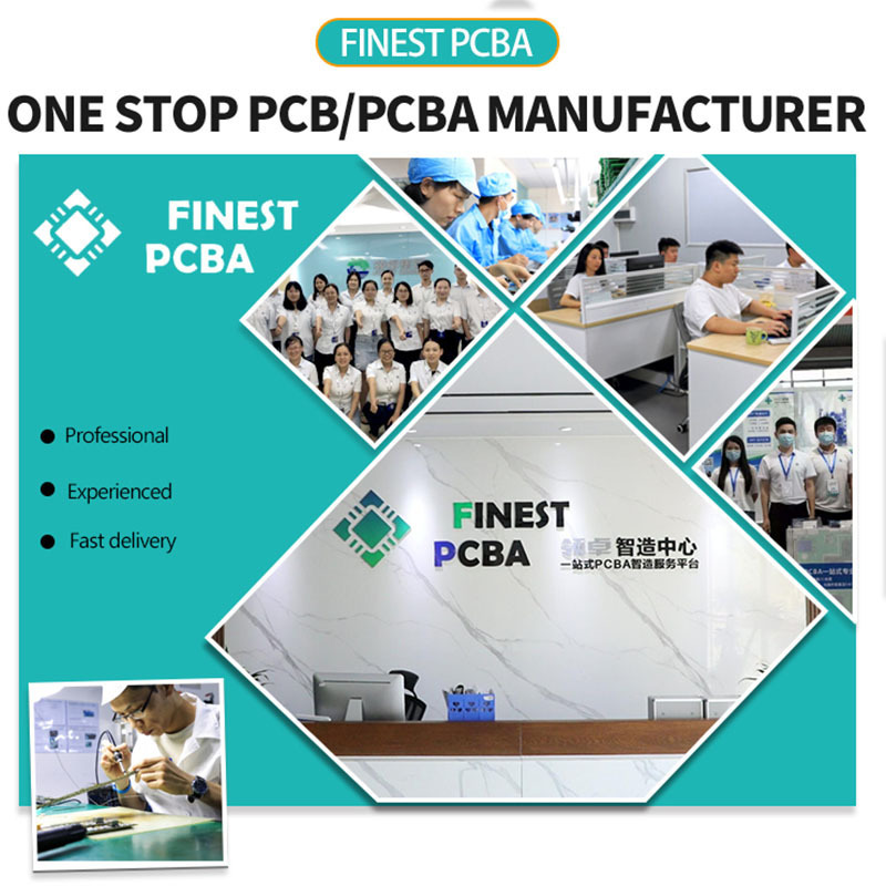
We are professional aluminum PCB board manufacture in Shenzhen,with a plant area of 2500m' and 8 SMT production lines. Equipped with new imported Hanwha 471,481,482,automatic solder.paste printers, ten-temperature zone reflowsoldering, wave soldering and other high-techequipments like X-RAY for BGA board.,, offer not only original electronic component scourcing service and our own factory PCB board, but also offer PCBA assembly service , especially customized in LED SMD, we have large amount of customers all over the world as below, if you have any request for LED assembly, please let us know your detail.
Finest PCB Assembly Limited is also a subsidiary of FINEST Group, which was established in April 2003, focusing on PCB board manufacturing, SMT processing, and component support services. In April 2019, we set up Finest SMT factory, specializing in EMS processing, fast SMT proofing, and small batch production. With the ability of material selection, sample making, small batch production, and testing services, we are capable to improve the efficiency of research and development to provide faster services.
Why Choonese Us
|
Delivery Time
|
Normal Delivery Time:
|
24 hours ( fastest 12 hours quick-turn)
|
|
|
||
|
|
Small Production:
|
72 hours( fastest 24 hours quick-turn)
|
|
|
||
|
|
Medium Production:
|
5 working days
|
|
|
||
|
Capacity
|
SMT assembly
|
500W point/day
|
|
|
||
|
|
THT assembly
|
30W point/day
|
|
|
||
|
Components
|
A full set of substitute materials
|
Have a mature component procurement management system, and provide cost-effective services for OEM projects.
|
|
|
||
|
|
Only SMT
|
Do SMT and backhand welding according to components and PCB boards provided by customers.
|
|
|
||
|
|
Components purchasing
|
Customers provide core components, and we provide substituting services for other components
|
|
|
||
|
PCB Capability
|
|
|
|
|
|
Attribute: see (*) below as applies
|
S/Sided
|
D/Sided
|
Multilayer
|
Advanced
|
|
Minimum Line/Spacing, Internal Layer
|
N/A
|
N/A
|
.004”/.004”
|
.003”/.003”
|
|
Minimum Line/Spacing, External Layer
|
.007”/.008”
|
.007”/.008”
|
.005”/.005”
|
.003”/.003”
|
|
Aspect Ratio (Thickness to Drill)
|
6:1
|
6:1
|
8:1
|
10:1
|
|
Minimum Drilled Hole Size
|
.010”
|
.008”
|
.008”
|
.008”
|
|
Land Size Internal (Diameter Over Drill)
|
N/A
|
N/A
|
.015”
|
.012”
|
|
Land size External (Diameter Over Drill)
|
.012”
|
.012”
|
.012”
|
.010”
|
|
Plane Clearance (Diameter Over Drill)
|
.030”
|
.030”
|
.030”
|
.024”
|
|
Plated Hole Tolerance
|
+/- .003”
|
+/- .003”
|
+/- .003”
|
+/- .002”
|
|
Minimum Dielectric Thickness
|
N/A
|
N/A
|
.0025”
|
.002”
|
|
Minimum Core Thickness
|
N/A
|
N/A
|
.004”
|
.003”
|
|
Minimum PCB Thickness **
|
.017”
|
.018”
|
.020”
|
.020”
|
|
Maximum PCB Thickness
|
.125”
|
.125”
|
.250”
|
.250”
|
|
Thickness Tolerance (%)
|
+/- 10
|
+/- 10
|
+/- 10
|
+/- 5
|
|
Maximum Board Dimensions *
|
16” x 52”*
|
19” x 22”*
|
17” x 23”*
|
17” x 23”*
|
|
Fabrication Tolerances (overall dimension)
|
+/- .010”
|
+/- .010”
|
+/- .010”
|
+/- .005”
|
|
Bow and Twist (Through Hole) %
|
1.5
|
1.5
|
1.5
|
1
|
|
Bow and Twist (SMT) %
|
.75
|
.75
|
.75
|
.75
|
|
Minimum Conductor to Edge
|
.015”
|
.015”
|
.015”
|
.010”
|
|
Layer to Layer Registration Tolerance
|
N/A
|
.004”
|
.004”
|
.003”
|
|
Component Pitch
|
.025”
|
.025”
|
.025”
|
.015”
|
|
Soldermask Clearance
|
.005”
|
.005”
|
.005”
|
.004”
|
|
Soldermask Dams
|
.005”
|
.005”
|
.005”
|
.004”
|
|
Impedance Tolerance (>50 Ohms) %
|
+/- 10
|
+/- 10
|
+/- 10
|
+/- 8
|
|
Maximum Layers
|
1
|
1
|
12
|
16
|
|
Minimum Copper Weight Inners (oz.)
|
N/A
|
N/A
|
|
1/4
|
|
Maximum Copper Weight Int. Ground (oz.)
|
N/A
|
N/A
|
3
|
8
|
|
Maximum Copper Weight Int. Signal (oz.)
|
N/A
|
N/A
|
2
|
6
|
|
Maximum Copper Weight Ext. Ground (oz.)
|
4
|
4
|
2
|
10
|
|
Maximum Copper Weight Ext. Signal (oz.)
|
4
|
4
|
3
|
10
|
|
PCBA Technical Capability
|
|
|
1. Assembly Type::
|
FR4, FPC, Rigid-flex PCB, Metal base PCB.
|
|
2. Assembly Specification:
|
Min size L50*W50mm; Max size: L510*460mm
|
|
3. Assembly thickness:
|
Min thickness: 0.2mm; Max thickness: 3.0mm
|
|
4. Components Specification
|
|
|
Components DIP:
|
01005Chip/0.35 Pitch BGA
|
|
Minimum device accurace:
|
+/-0.04mm
|
|
Minimum footprint distance:
|
0.3mm
|
|
5. File format:
|
BOM list; PCB Gerber file:
|
|
6. Test
|
|
|
IQC:
|
Incoming inspection
|
|
IPQC:
|
Production inspection; first ICR test
|
|
Visual QC:
|
Regularly quality inspection
|
|
SPI test :
|
Automatic solder paste optical inspection
|
|
AOI:
|
SMD component welding detection, components shortage & component polarity detection
|
|
X-Ravd:
|
BGA test; QFN and other precision devices hidden PAD device inspection
|
|
Function test:
|
Test function and performance according to customer's test procedures and steps
|
|
7. Reworking:
|
BGA rework equipment
|
|
8. Delivery Time
|
|
|
Normal delivery time:
|
24 hours( fastest 12 hours quick-turn)
|
|
Small production:
|
72 hours( fastest 24 hours quick-turn)
|
|
Medium production:
|
5 working davs.
|
|
9. Capacity:
|
SMT assembly 5 million point/day;plug-in & welding 300,000 point/day; 50-100 items/day
|
|
10. Components Service
|
|
|
A full set of substitute materials:
|
Have a experience component procurement sourcing, management system, and provide cost-effective services for OEM projects
|
|
Only SMT:
|
Do SMT and backhand welding according to components PCB boards provided by customers.
|
|
Components purchasing:
|
Customers provide core components, and we provide components sourcing services.
|
FAQ
1, ARE YOU A FACTORY OR TRADE COMPANY?-FINEST is a PCB manufacturer with three factories.
2, WHAT PAYMENT TERMS DO YOU ACCEPT?
-T/T, West Union, D/A, samples accept Paypal.
3, WHAT DELIVERY TERMS COULD YOU DO?
-FOB Shenzhen, FOB HK, CFR, CIF, DDU.
4, DO YOU HAVE MOQ?
-No. But for orders less than 3s.q.m. set up cost will be charged.
5, WHAT IS YOUR STANDARD LEAD TIME?
-Samples: 3~5 days (1L~4L), 5~8 working days >6L
Middle volume production (less than 200 s.q.m): 7~8 working days for 1L and 2L, 8~15 working days for multilayer
Big volume production:15~20 working days.
FAQ
1. who are we?
We are based in Guangdong, China, start from 2019,sell to Domestic Market(50.00%),North America(15.00%),South America(12.00%),Northern Europe(12.00%),Western Europe(5.00%),Southeast Asia(2.00%),Mid East(2.00%),Eastern Europe(2.00%). There are total about 301-500 people in our office.
2. how can we guarantee quality?
Always a pre-production sample before mass production;
Always final Inspection before shipment;
3.what can you buy from us?
PCBA,PCB Assembly,PCBA Board,LED PCBA,Electronic PCBA
4. why should you buy from us not from other suppliers?
*A 18-year one-stop solution provider *Strong R&D group with 30 engineers *Monthly output:45000 sqm of PCBs and PCBAs *4500-square-meter factory *Eight SMT production-line *Automatic SMT, Reflow machine, AOI&x-RAY *Fast response, reply within 24hrs
5. what services can we provide?
Accepted Delivery Terms: FOB,CIF,EXW,Express Delivery;
Accepted Payment Currency:USD,EUR,GBP;
Accepted Payment Type: T/T,L/C,MoneyGram,Western Union;
Language Spoken:English,French
Hot Searches
