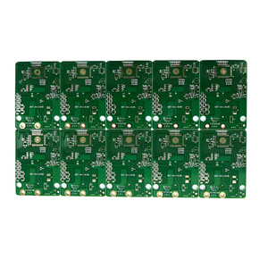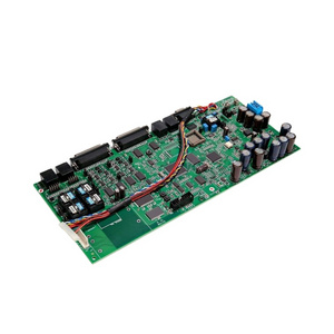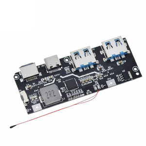
- Product Details
- {{item.text}}
Quick Details
-
Place of Origin:
-
Guangdong, China
-
Brand Name:
-
POE
-
Copper Thickness:
-
1OZ, 0.5OZ-6OZ
-
Min. Hole Size:
-
0.20mm
-
Min. Line Width:
-
4mil
-
Min. Line Spacing:
-
4mil
-
Surface Finishing:
-
Hasl Lead Free
-
Board Size:
-
500*500
-
Color:
-
Green
-
Min Solder Mask Bridge:
-
≥0.08mm
-
Aspect ratio:
-
15:1
-
Minimum Annular ring:
-
4mil
-
Impedence Control Tolerance:
-
±5%
-
Service:
-
PCB&PCBA
-
PCB:
-
Customized
-
MOQ:
-
1
-
Customize:
-
Avaliable
Quick Details
-
Base Material:
-
FR4
-
Board Thickness:
-
1.6mm
-
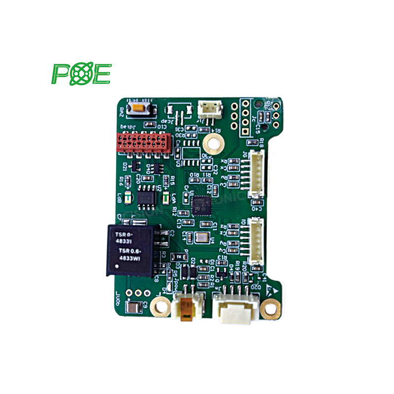
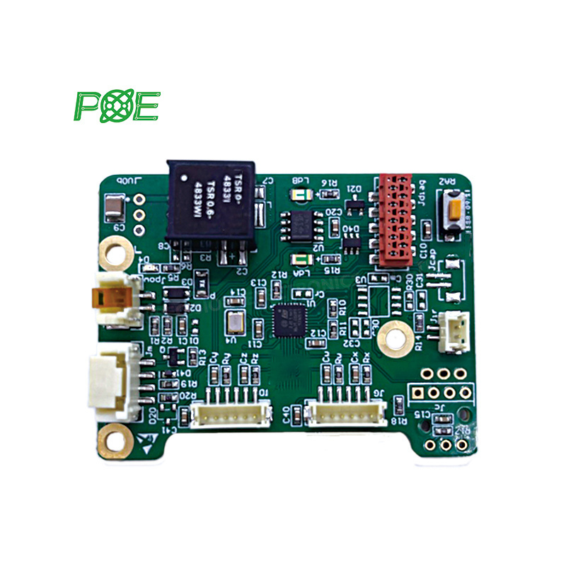
Model Number:
-
POE-PCBA-09797
-
Place of Origin:
-
Guangdong, China
-
Brand Name:
-
POE
-
Copper Thickness:
-
1OZ, 0.5OZ-6OZ
-
Min. Hole Size:
-
0.20mm
-
Min. Line Width:
-
4mil
-
Min. Line Spacing:
-
4mil
-
Surface Finishing:
-
Hasl Lead Free
-
Board Size:
-
500*500
-
Color:
-
Green
-
Min Solder Mask Bridge:
-
≥0.08mm
-
Aspect ratio:
-
15:1
-
Minimum Annular ring:
-
4mil
-
Impedence Control Tolerance:
-
±5%
-
Service:
-
PCB&PCBA
-
PCB:
-
Customized
-
MOQ:
-
1
-
Customize:
-
Avaliable

POE PCB manufacturing capabilities
|
Item |
PCB Capability |
|
|
1.Base Material |
FR-4 / High TG FR-4 / Lead free Materials (ROHS Compliant) / Halogen Free material /CEM-3/CEM-1/ /PTFE/ROGERS/ARLON/TACONIC |
|
|
2.Layers |
1-40 |
|
|
3.Finised inner/outer copper thickness |
1-6OZ |
|
|
4.Finished board thickness |
0.2-7.0mm |
|
|
Tolerance |
Board thickness≤1.0mm: +/-0.1mm 1<Board thickness≤2.0mm: +/-10% Board thickness>2.0mm: +/-8% |
|
|
5.Max panel size |
≤2sidesPCB: 600*1500mm Multilayer PCB: 500*1200mm |
|
|
6.Min conductor line width/spacing |
Inner layers: ≥3/3mil Outer layers: ≥3.5/3.5mil |
|
|
7.Min hole size |
Mechanical hole: 0.15mm Laser hole: 0.1mm |
|
|
Drilling precision: first drilling |
First drilling: 1mil Second drilling: 4mil |
|
|
8.Warpage |
Board thickness≤0.79mm: β≤1.0% 0.80≤Board thickness≤2.4mm: β≤0.7% Board thickness≥2.5mm: β≤0.5% |
|
|
9.Controlled Impedance |
+/-5% |
|
|
10. Aspect Ratio |
15:1 |
|
|
11.Min welding ring |
4mil |
|
|
12.Min solder mask bridge |
≥0.08mm |
|
|
13.Plugging vias capability |
0.2-0.8mm |
|
|
14. Hole tolerance |
PTH: +/-3mil NPTH: +/-2mil |
|
|
15.Outline profile |
Rout/ V-cut/ Bridge/ Stamp hole |
|
|
16.Surface treatment |
OSP: 0.5-0.5um HASL: 2-40um Lead free HASL: 2-40um ENIG: Au 1-10U’’ ENEPIG: PB 2-5U’’/ Au 1-8U’’ Immersion Tin:0.8-1.2um Immersion silver: 0.1-1.2um Peelable blue mask Carbon ink Gold plating: Au 1-150U’’ |
|
|
17. E-testing pass percent |
97% pass for the first time,+/-2%(tolerance) |
|
|
FQC-Physical Lab: Reliability tests |
||
|
18.Certificate |
ROHS, ISO9001:2015, ISO13484:2016, IPC3 Standard |
|
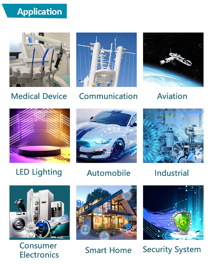
Application Fields
We produce PCBs for our customers working in frequency ranges from LED products to communication equipments and in industries as diverse as Medical devices through to automotive, and aerospace etc