- Product Details
- {{item.text}}
Quick Details
-
Supplier Type:
-
circuit board assembly Manufacturer
-
Copper Thickness:
-
0.5-3oz
-
Layer:
-
1-16
-
regular Board thickness:
-
0.8/1.0/1.2/1.5/1.6/2.0mm
-
Assembly Type:
-
FR4, FPC, Rigid-flex PCB, Metal base PCB
-
Assembly Specification:
-
Min size L50*W50mm; Max size: L510*460mm
-
Assembly thickness:
-
Min thickness: 0.2mm; Max thickness: 3.0mm
-
Minimum device accuracy:
-
+/-0.04mm
-
Minimum footprint distance:
-
0.3mm
-
Capacity:
-
SMT 500W point/day;THT 30W point/day
-
Certificate:
-
ROHS/ISO9001
-
Keywords:
-
pcba cutcuit
Quick Details
-
Model Number:
-
PCB Assembly
-
Place of Origin:
-
Guangdong, China
-
Brand Name:
-
FINEST
-
Supplier Type:
-
circuit board assembly Manufacturer
-
Copper Thickness:
-
0.5-3oz
-
Layer:
-
1-16
-
regular Board thickness:
-
0.8/1.0/1.2/1.5/1.6/2.0mm
-
Assembly Type:
-
FR4, FPC, Rigid-flex PCB, Metal base PCB
-
Assembly Specification:
-
Min size L50*W50mm; Max size: L510*460mm
-
Assembly thickness:
-
Min thickness: 0.2mm; Max thickness: 3.0mm
-
Minimum device accuracy:
-
+/-0.04mm
-
Minimum footprint distance:
-
0.3mm
-
Capacity:
-
SMT 500W point/day;THT 30W point/day
-
Certificate:
-
ROHS/ISO9001
-
Keywords:
-
pcba cutcuit

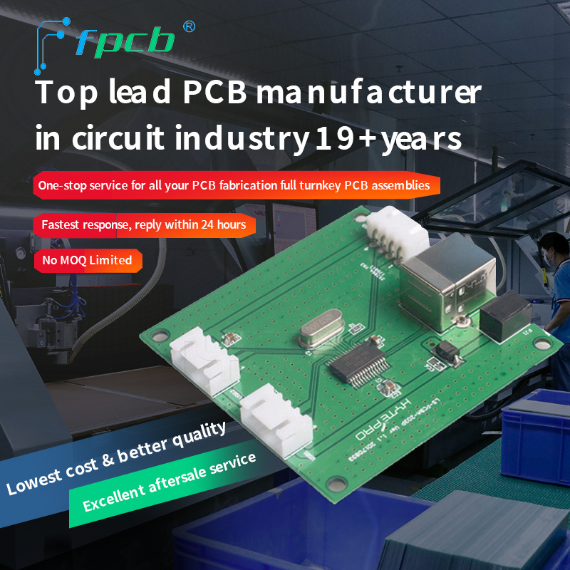
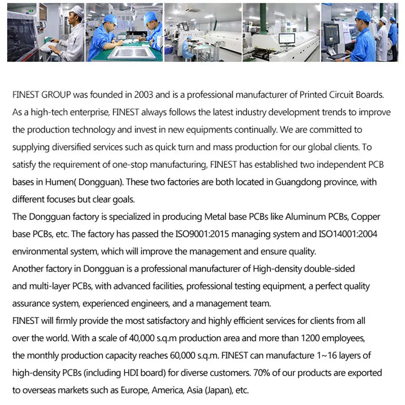
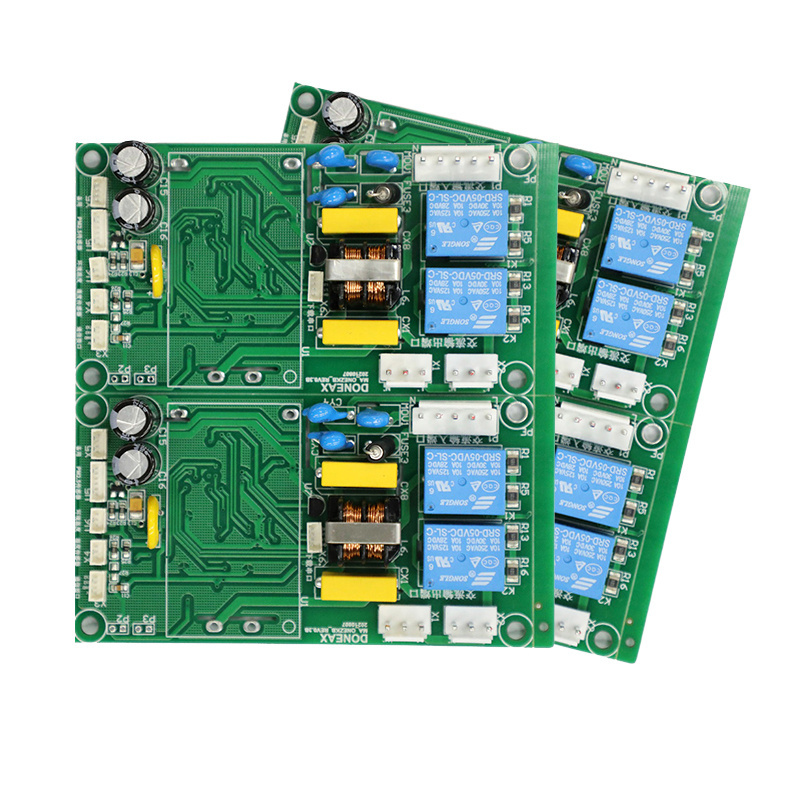
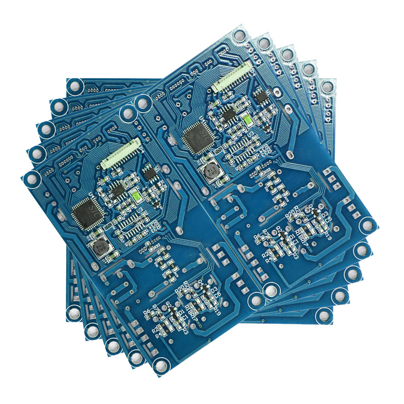
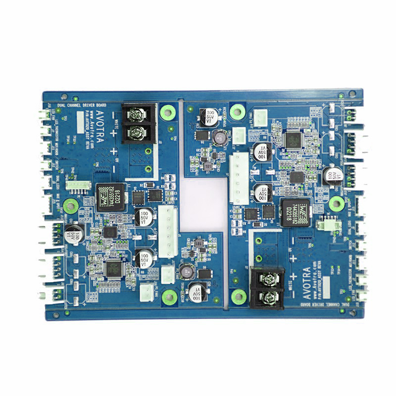
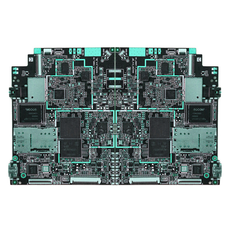
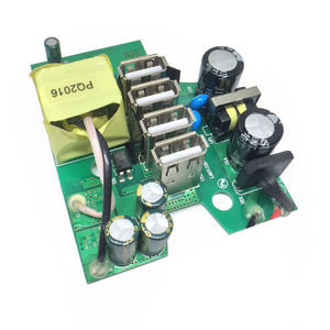
We are professional aluminum PCB board manufacture in Shenzhen,with a plant area of 2500m' and 8 SMT production lines. Equipped with new imported Hanwha 471,481,482,automatic solder.paste printers, ten-temperature zone reflowsoldering, wave soldering and other high-techequipments like X-RAY for BGA board.,, offer not only original electronic component scourcing service and our own factory PCB board, but also offer PCBA assembly service , especially customized in LED SMD, we have large amount of customers all over the world as below, if you have any request for LED assembly, please let us know your detail.
Why Choonese Us
|
Delivery Time
|
Normal Delivery Time:
|
24 hours ( fastest 12 hours quick-turn)
|
|
|
||
|
|
Small Production:
|
72 hours( fastest 24 hours quick-turn)
|
|
|
||
|
|
Medium Production:
|
5 working days
|
|
|
||
|
Capacity
|
SMT assembly
|
500W point/day
|
|
|
||
|
|
THT assembly
|
30W point/day
|
|
|
||
|
Components
|
A full set of substitute materials
|
Have a mature component procurement management system, and provide cost-effective services for OEM projects.
|
|
|
||
|
|
Only SMT
|
Do SMT and backhand welding according to components and PCB boards provided by customers.
|
|
|
||
|
|
Components purchasing
|
Customers provide core components, and we provide substituting services for other components
|
|
|
||
|
PCB Capability
|
|
|
|
|
|
Attribute: see (*) below as applies
|
S/Sided
|
D/Sided
|
Multilayer
|
Advanced
|
|
Minimum Line/Spacing, Internal Layer
|
N/A
|
N/A
|
.004”/.004”
|
.003”/.003”
|
|
Minimum Line/Spacing, External Layer
|
.007”/.008”
|
.007”/.008”
|
.005”/.005”
|
.003”/.003”
|
|
Aspect Ratio (Thickness to Drill)
|
6:1
|
6:1
|
8:1
|
10:1
|
|
Minimum Drilled Hole Size
|
.010”
|
.008”
|
.008”
|
.008”
|
|
Land Size Internal (Diameter Over Drill)
|
N/A
|
N/A
|
.015”
|
.012”
|
|
Land size External (Diameter Over Drill)
|
.012”
|
.012”
|
.012”
|
.010”
|
|
Plane Clearance (Diameter Over Drill)
|
.030”
|
.030”
|
.030”
|
.024”
|
|
Plated Hole Tolerance
|
+/- .003”
|
+/- .003”
|
+/- .003”
|
+/- .002”
|
|
Minimum Dielectric Thickness
|
N/A
|
N/A
|
.0025”
|
.002”
|
|
Minimum Core Thickness
|
N/A
|
N/A
|
.004”
|
.003”
|
|
Minimum PCB Thickness **
|
.017”
|
.018”
|
.020”
|
.020”
|
|
Maximum PCB Thickness
|
.125”
|
.125”
|
.250”
|
.250”
|
|
Thickness Tolerance (%)
|
+/- 10
|
+/- 10
|
+/- 10
|
+/- 5
|
|
Maximum Board Dimensions *
|
16” x 52”*
|
19” x 22”*
|
17” x 23”*
|
17” x 23”*
|
|
Fabrication Tolerances (overall dimension)
|
+/- .010”
|
+/- .010”
|
+/- .010”
|
+/- .005”
|
|
Bow and Twist (Through Hole) %
|
1.5
|
1.5
|
1.5
|
1
|
|
Bow and Twist (SMT) %
|
.75
|
.75
|
.75
|
.75
|
|
Minimum Conductor to Edge
|
.015”
|
.015”
|
.015”
|
.010”
|
|
Layer to Layer Registration Tolerance
|
N/A
|
.004”
|
.004”
|
.003”
|
|
Component Pitch
|
.025”
|
.025”
|
.025”
|
.015”
|
|
Soldermask Clearance
|
.005”
|
.005”
|
.005”
|
.004”
|
|
Soldermask Dams
|
.005”
|
.005”
|
.005”
|
.004”
|
|
Impedance Tolerance (>50 Ohms) %
|
+/- 10
|
+/- 10
|
+/- 10
|
+/- 8
|
|
Maximum Layers
|
1
|
1
|
12
|
16
|
|
Minimum Copper Weight Inners (oz.)
|
N/A
|
N/A
|
|
1/4
|
|
Maximum Copper Weight Int. Ground (oz.)
|
N/A
|
N/A
|
3
|
8
|
|
Maximum Copper Weight Int. Signal (oz.)
|
N/A
|
N/A
|
2
|
6
|
|
Maximum Copper Weight Ext. Ground (oz.)
|
4
|
4
|
2
|
10
|
|
Maximum Copper Weight Ext. Signal (oz.)
|
4
|
4
|
3
|
10
|
|
PCBA Technical Capability
|
|
|
1. Assembly Type::
|
FR4, FPC, Rigid-flex PCB, Metal base PCB.
|
|
2. Assembly Specification:
|
Min size L50*W50mm; Max size: L510*460mm
|
|
3. Assembly thickness:
|
Min thickness: 0.2mm; Max thickness: 3.0mm
|
|
4. Components Specification
|
|
|
Components DIP:
|
01005Chip/0.35 Pitch BGA
|
|
Minimum device accurace:
|
+/-0.04mm
|
|
Minimum footprint distance:
|
0.3mm
|
|
5. File format:
|
BOM list; PCB Gerber file:
|
|
6. Test
|
|
|
IQC:
|
Incoming inspection
|
|
IPQC:
|
Production inspection; first ICR test
|
|
Visual QC:
|
Regularly quality inspection
|
|
SPI test :
|
Automatic solder paste optical inspection
|
|
AOI:
|
SMD component welding detection, components shortage & component polarity detection
|
|
X-Ravd:
|
BGA test; QFN and other precision devices hidden PAD device inspection
|
|
Function test:
|
Test function and performance according to customer's test procedures and steps
|
|
7. Reworking:
|
BGA rework equipment
|
|
8. Delivery Time
|
|
|
Normal delivery time:
|
24 hours( fastest 12 hours quick-turn)
|
|
Small production:
|
72 hours( fastest 24 hours quick-turn)
|
|
Medium production:
|
5 working davs.
|
|
9. Capacity:
|
SMT assembly 5 million point/day;plug-in & welding 300,000 point/day; 50-100 items/day
|
|
10. Components Service
|
|
|
A full set of substitute materials:
|
Have a experience component procurement sourcing, management system, and provide cost-effective services for OEM projects
|
|
Only SMT:
|
Do SMT and backhand welding according to components PCB boards provided by customers.
|
|
Components purchasing:
|
Customers provide core components, and we provide components sourcing services.
|
FAQ
1, ARE YOU A FACTORY OR TRADE COMPANY?-FINEST is a PCB manufacturer with three factories.
2, WHAT PAYMENT TERMS DO YOU ACCEPT?
-T/T, West Union, D/A, samples accept Paypal.
3, WHAT DELIVERY TERMS COULD YOU DO?
-FOB Shenzhen, FOB HK, CFR, CIF, DDU.
4, DO YOU HAVE MOQ?
-No. But for orders less than 3s.q.m. set up cost will be charged.
5, WHAT IS YOUR STANDARD LEAD TIME?
-Samples: 3~5 days (1L~4L), 5~8 working days >6L
Middle volume production (less than 200 s.q.m): 7~8 working days for 1L and 2L, 8~15 working days for multilayer
Big volume production:15~20 working days.
Hot Searches
