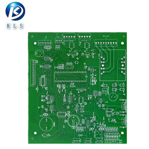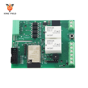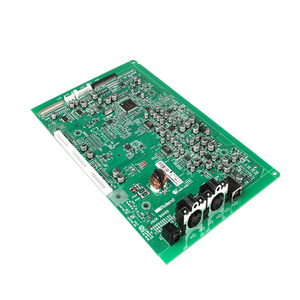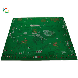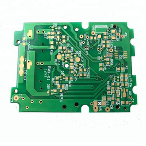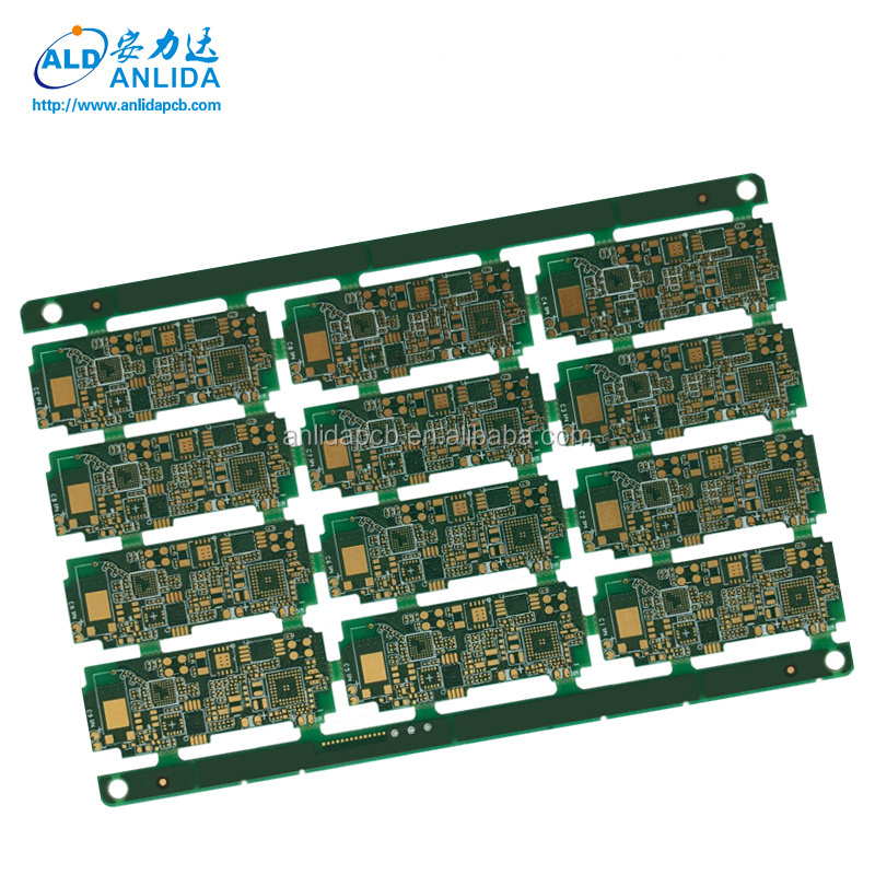
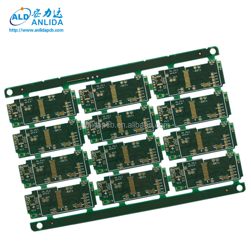
- Product Details
- {{item.text}}
Quick Details
-
Place of Origin:
-
Guangdong, China
-
Brand Name:
-
anlidapcb
-
Copper Thickness:
-
0.5oz-1oz
-
Min. Hole Size:
-
0.10mm
-
Min. Line Width:
-
0.076mm/3mil
-
Min. Line Spacing:
-
0.076mm/3mil
-
Surface Finishing:
-
ENIG
-
Board Size:
-
Green
-
Impedance control:
-
50/90±10% ohm
-
Number of Layers:
-
6 Layers
-
Product application:
-
Wireless transmission
-
Main service:
-
design fabrication assembly
-
TG Value:
-
TG150-TG180
-
Product design:
-
anlida design
-
shenzhen pcb:
-
One stop service
-
Flame Resistance:
-
94v0
-
Standard:
-
IPC-A-610G CLASS II
-
Product name:
-
dark green circuit board
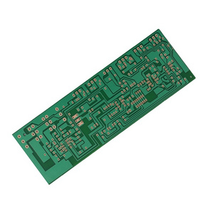
Quick Details
-
Base Material:
-
FR-4
-
Board Thickness:
-
0.6mm
-
Model Number:
-
H-21
-
Place of Origin:
-
Guangdong, China
-
Brand Name:
-
anlidapcb
-
Copper Thickness:
-
0.5oz-1oz
-
Min. Hole Size:
-
0.10mm
-
Min. Line Width:
-
0.076mm/3mil
-
Min. Line Spacing:
-
0.076mm/3mil
-
Surface Finishing:
-
ENIG
-
Board Size:
-
Green
-
Impedance control:
-
50/90±10% ohm
-
Number of Layers:
-
6 Layers
-
Product application:
-
Wireless transmission
-
Main service:
-
design fabrication assembly
-
TG Value:
-
TG150-TG180
-
Product design:
-
anlida design
-
shenzhen pcb:
-
One stop service
-
Flame Resistance:
-
94v0
-
Standard:
-
IPC-A-610G CLASS II
-
Product name:
-
dark green circuit board
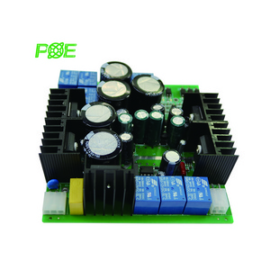
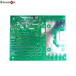
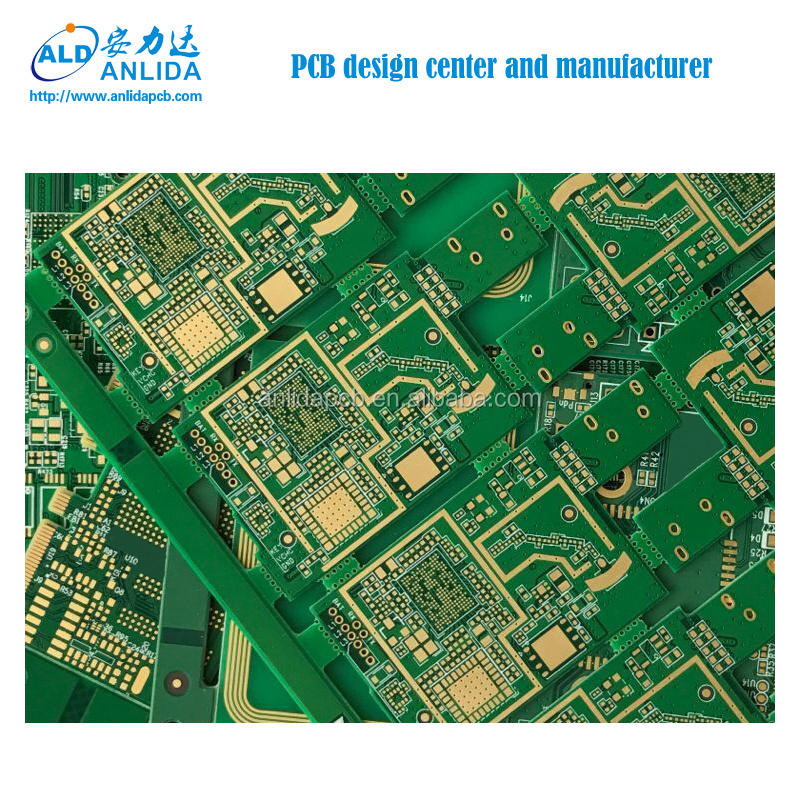
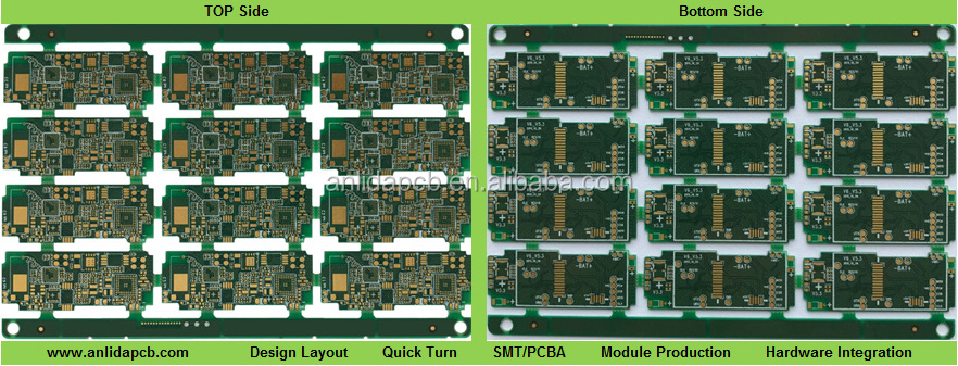
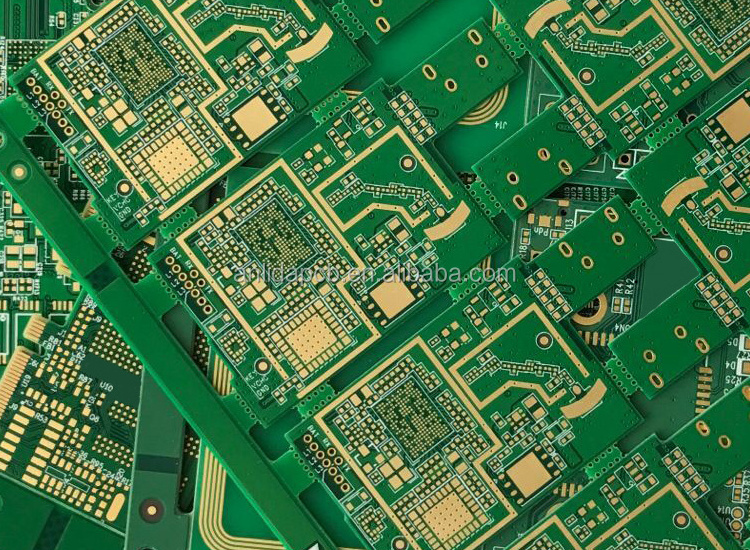
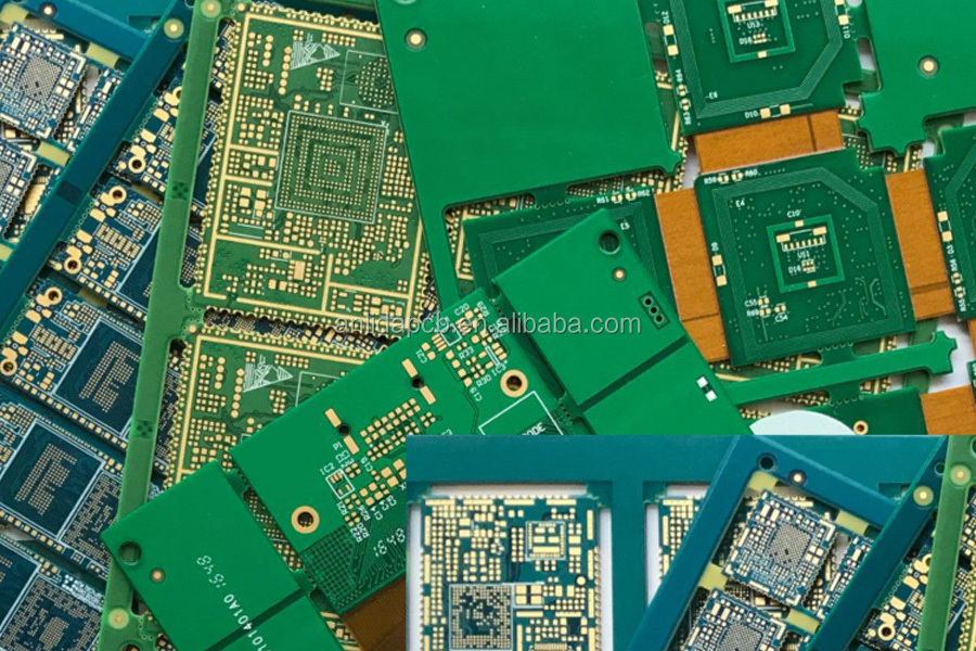
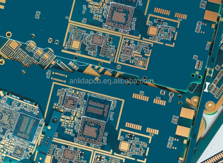
Dark green 6 Layers 94v0 pcb printed pcb circuit board :
We have been focusing on rapid manufacturing services for samples, small and medium-scale PCBs; Meantime, we have established a complete quality control system to ensure the products with zero failed rate. In order to meet the demand of medium and high-end and special products, we added two production lines for samples in 2014, and we can achieve rapid production to the greatest extent.
We have the professional teams for market, engineering technology and quality management. From production to shipment, we provide customers with timely, accurate, fast and excellent services. High quality and best price are the biggest advantages of our team. Strong sense of responsibility, rigorous design, attention to detail, and zero failed rate are our continuous goals.
Professional team, professional staff, professional services
- HDI board 5+N+5 1.5mil/1.5mil trace and spacing .4mil laser drll,resin filled and copper plating fill
- Athena and RF board with PTEE material(Rogers,Teconic,RT5880)-Have material in stock
- Counter sink,edge Control depth
- Via in pad filled and planerized with copper
- ENEPIG,soft gold,hard gold,Gold finger,Flash gold and orther normal finish
- Rigid-flex and flex board
- 5G board with TU 872-LK or other good material
- Layout service ,layout team has about 30 engineers,engineer has over 10 years experience.Use ALLEGRO V15 16 and16.5;MENTOR VX2.1 and7.9.5; AD
- Heavy Copper up to 12 OZ
- Big board size up to 35inch(1.37meter,2 layer)30inch(1.18meter,multilayer)
- Max,layer count 42
- Max,board thickness 12MM
- Burn in board ,ATE board,Load board,DUT board
- MIN pitch 0.35mm
- Rogers and FR-4 TG170 / TG180 material lamination
- Back drill
- Buired&blind via hole board,4 times lamination
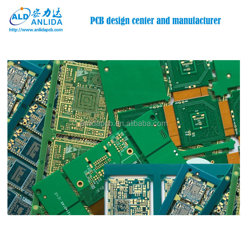
Company Introduction:
All Services:
- High-Speed PCB Design / PCB Layout
- High-Speed PCB SI / PI / EMC Analysis
- Fast 1-24LPCB Prototype,samll-medium volume Fabrication
- Professional HDI PCB Production
- Rigid-Flex Board Manufacture
- SMT Assembly / PCBA Assembly
- PCB Parts Sourcing
PCB-parameters:
Printed Circuit Board Production:
| NO. | Item | Prototype | Mass Production |
| 1 | Layer Count | 1-30 Layers | 1-20 Layers |
| 2 | Max Panel Size | ≤1000X1000mm | ≤700X700mm |
| 3 | Base Material Type | FR4,High Tg FR4, Rogers,Halogen Free | FR4,High Tg FR4, Rogers,Halogen Free |
| 4 | Max Board Thickness | ≤10 mm | ≤10 mm |
| 5 | Min Board Thickness |
2L≥0.2mm,4L≥ 0.3mm
6L≥0.4mm,8L≥0.6mm 10L≥0.65mm,12L≥0.8mm |
2L≥0.2mm,4L≥ 0.3mm
6L≥0.4mm,8L≥0.6mm 10L≥0.65mm,12L≥0.8mm |
| 6 | Min Line Width | ≥ 0.05mm(2mil) | ≥ 0.064mm(2.5mil) |
| 7 | Min Line Space | ≥ 0.064mm(2.5mil) | ≥0.075mm(3mil) |
| 8 | Min Through hole | 0.15mm(6mil) | 0.15mm(6mil) |
| 9 | Min Blind hole | 0.1mm(4mil) | 0.1mm(4mil) |
| 10 | Min Buried Hole | 0.2mm(8mil) | 0.2mm(8mil) |
| 11 | Min Plated Hole Thickness | 20µm(0.8mil) | 20µm(0.8mil) |
| 12 | Surface coating | HASL,ENIG, OSP,ENIG+OSP,Plating Ni/Au/Ag | HASL,ENIG, OSP,ENIG+OSP,Plating Ni/Au/Ag |
| 13 | Solder Mask color | Green,Blue,Black,White,Yellow,Red | Green,Blue,Black,White,Yellow,Red |
| 14 | Silkscreen color | White,Black,Yellow,Red, | White,Black,Yellow,Red, |
| 15 | Thick Copper | 6oz/210µm | 4oz/140µm |
| 16 | MIN S/M Pitch | 0.1mm(4mil) | 0.1mm(4mil) |
| 17 | PTH Dia Tolerance | ±0.076mm(±3mil) | ±0.076mm(±3mil) |
| 18 | NPTH Dia Tolerance | ±0.05mm(±2mil) | ±0.05mm(±2mil) |
| 19 | Hole Position Deviation | ±0.05mm(±2mil) | ±0.05mm(±2mil) |
| 20 | Outline Tolerance | ±0.15mm (±6mil) | ±0.15mm (±6mil) |
| 21 | Controlled Impedance | +/-5% | +/-10% |
| 22 | WARP and TWIST | ≤0.75% | ≤0.75% |
| 23 | Flammability Class | 94V-0 | 94V-0 |
| 24 | Solderability test | 255 ℃ +/-5℃ | 255 ℃ +/-5℃ |
| 25 | Thermal stress | 288+5℃,10Sec | 288+5℃,10Sec |
| 26 | Test Voltage | 50-330V | 50-330V |
| 27 | Adhesion Test | NO PEELING | NO PEELING |
| 28 | Other Inspection item | IPC-6012 / A-600H | IPC-6012 / A-600H |
flow diagram: