- Product Details
- {{item.text}}
Quick Details
-
Software customization:
-
Yes
-
Description:
-
Yes
-
Degree of completion:
-
full complete
-
Finished product Type:
-
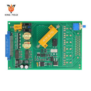
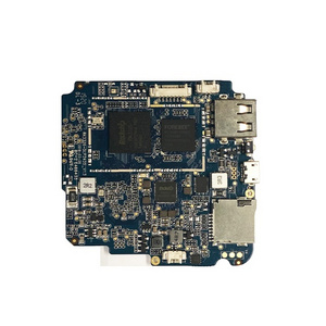
PCBA
-
Province:
-
Guangdong
Quick Details
-
Place of Origin:
-
Guangdong, China
-
Brand Name:
-
OEM
-
Model Number:
-
202401061
-
Software customization:
-
Yes
-
Description:
-
Yes
-
Degree of completion:
-
full complete
-
Finished product Type:
-
PCBA
-
Province:
-
Guangdong
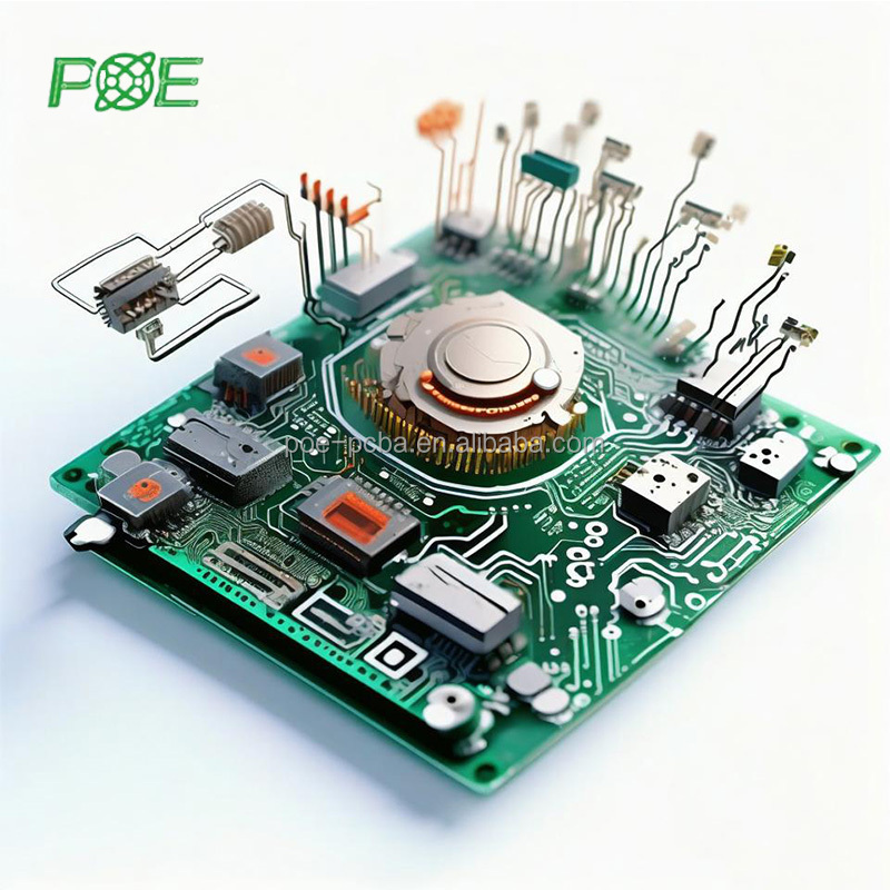
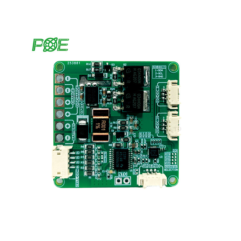
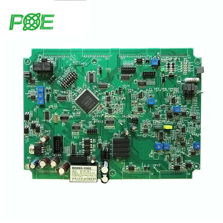
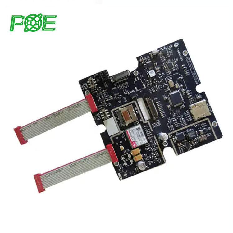
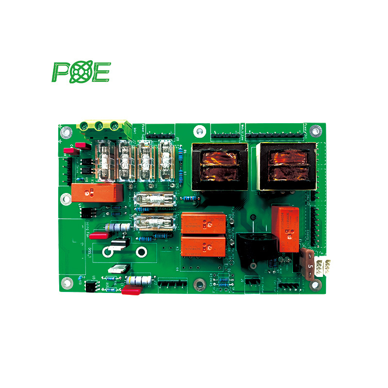
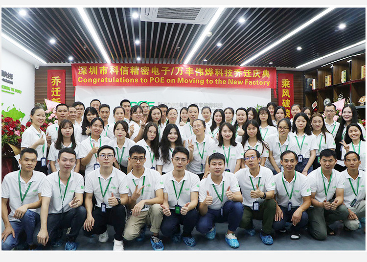
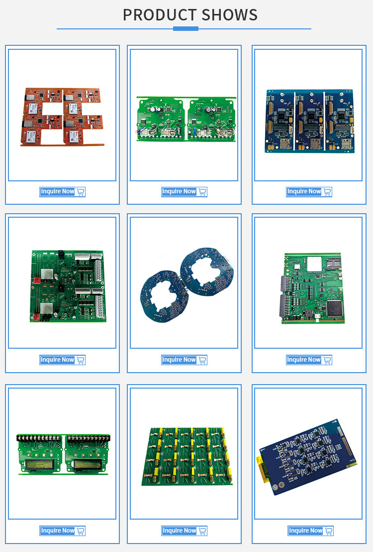
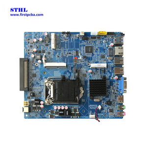
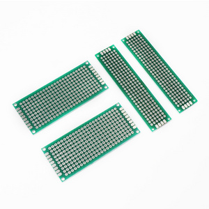
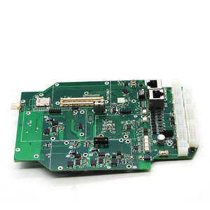
One of the PCB assembly manufacturer, POE adopts advanced production techniques and manufacturing practices with specialization in a varied range of PCB fabrication process, producing high quality multi-layered PCB. With over 20 years of combined experience in rendering high tech PCB assembly and manufacturing services, we have the capability to manufacture pcb ranging from basic single sided boards up to 40 layer PCB ,and provide one stop turnkey services, including quick turn prototype, pcb manufacturing, SMT & DIP assembly, components sourcing, function test, cable harness and box assembled services and so on.
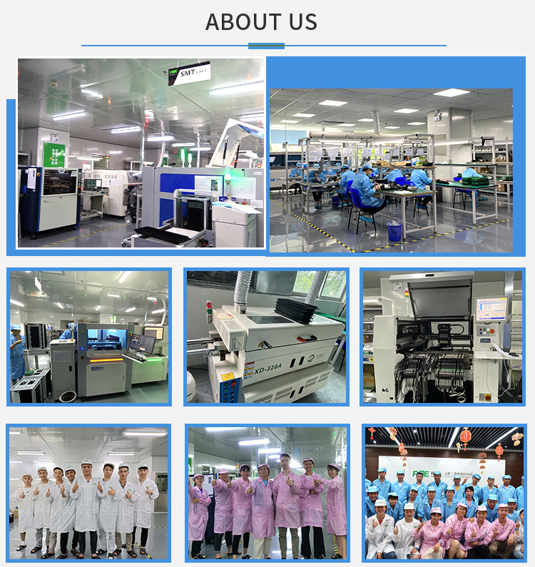
|
Products Description
|
|
|
||
|
Seq
|
Item
|
Capability
|
||
|
1
|
Base Material
|
FR-4, High TG FR-4, Halogen Free material, CEM-3, CEM-1, PTFE, Rogers, Arlon, Taconic, Aluminum base, PI, etc
|
||
|
2
|
Layers
|
1-40 L
|
||
|
3
|
Finished Inner/ Outer Copper Thickness
|
0.5-60Z
|
||
|
4
|
Finished Board Thickness
|
0.2-7. 0mm (s0.2mm needs review), ≤0 4mm for HASL
|
||
|
|
|
Board thicknesss1 .0mm: +/-0. 1mm
Board thickness>2 .0mm: +/-8%
|
||
|
5
|
Max Panel Size
|
≤2sidesPCB: 600*1500mm Multilayer PCB: 500*1200mm
|
||
|
6
|
Min Conductor Line Width/ Spacing
|
Inner layers:≥3/3mil
Outer layers: 23.5/3.5mil
|
||
|
7
|
Min Hole Size
|
Mechanical hole: 0. 15mm Laser hole: 0.1mm
|
||
|
|
|
Driling precision: first dilling First dilling: 1mil Second dilling: 4mil
|
||
|
8
|
Warpage
|
Board thicknesss0.79mm: β≤1.0% 0.80sBoard thicknesss2 4mm: βs0.7% Board thickness22 5mm: β≤0. 5%
|
||
|
9
|
Controlled Impedance
|
+/- 5 % 2(<502).+/-10%(2500),.>5002+/-5% (needs review)
|
||
|
10
|
Aspect Ratio
|
15:01
|
||
|
11
|
Min Welding Ring
|
4mil
|
||
|
12
|
Min Solder Mask Bridge
|
≥0.08mm
|
||
|
13
|
Plugging Vias Capability
|
0.2-0.8mm
|
||
|
14
|
Hole Tolerance
|
PTH: +/-3mil NPTH: +/-2mil
|
||
|
15
|
Outine Profile
|
Rout/ V-cut/ Bridge/ Stamp hole
|
||
|
16
|
Solder Mask Color
|
Green, yellow, black, blue, red, white, matte green
|
||
|
17
|
Component MarkColor
|
white, yellow, black
|
||
|
18
|
Surface Treatment
|
0SP.0.2-0.5um HASL:2-40um
Lead free HASL: 2-40um ENIG: Au 1-10U" ENEPIG: PB 2-5U"/ Au 1-8U" Immersion Tin:0.8-1 .5um Immersion silver:0.1-1 .2um Peelable blue mask Carbon ink Gold plating:Au 1-1 50U" |
||
|
19
|
E-Test
|
Flying probe tester:0.4-6.0mm, max 19.6*23.5inch
|
||
|
|
|
Min spacing from test pad to board edge:0.5 mm
|
||
|
|
|
Min conductive resistance:5 Q
|
||
|
|
|
Max insulation resistance:250 MQ
|
||
|
|
|
Max test voltage:500 V
|
||
|
|
|
Min test pad diameter:6 mil
|
||
|
|
|
Min test pad to pad spacing:10 mil
|
||
|
|
|
Max test current:200 MA
|
||
|
20
|
AOI
|
Orbotech SK-75 AOI:0.05-6.0mm, max 23.5*23.5inch
|
||
|
|
|
Orbotech Ves machine:0.05-6.0mm, max 23.5*23.5inch
|
||
|
21
|
ODM/ OEM Services
|
We have 6 SMT/ SMD production line and 2 DIP production line
|
||
FAQ
Q: What is needed for PCB/PCBA quotation?
A: For Bare PCB project, please provide Quantity, Gerber file and specification like material, surface finish treatment, copper thickness, board thickness, soldermask color and silkscreen color and other special specs.
For PCBA project, please provide above information as well, and BOM list, pick and place file. If you need turnkey service include programming and functional testing etc, kindly contact us for more details.
Q: Are my files safe?
A: Your files are held in complete safety and security.We protect the intellectual property for our customers in the whole process. All documents from customers are never shared with any third parties. We are willing to sign NDA effect by customer side local law and promising to keep customers data in high confidential level.
Q: What’s your minimum of quantity(MOQ) ?
A: There is no MOQ in POE (PCBA shenzhen). We are able to handle small as well as large volume production with flexibility.
Q: How to calculate the shipping cost?
A: The shipping cost is determined by the destination, weight, packing size of the goods. Please let us know if you need us to quote you the shipping cost.
Q: What other service do you have?
A: We mainly focus on PCB +Assembly +Components sourcing service. Additionally, we can also provide programming, testing, cables, enclosure assembly service.
Q: Can we inspect quality during production?
A: Yes, we are open and transparent on each production process. We Welcome you visit our factory to inspect our production process.
Q: What is your testing policy and how you control the quality?
A: Regarding to PCB samples, usually tested by flying probe; for PCB Volume over 3 square meters, usually tested by Electrical fixture which is faster. As to PCBA production, there are automated optical inspection (AOI) for each batch, X-ray inspection for BGA parts, first article inspection(FAI) before mass production.
Hot Searches
