- Product Details
- {{item.text}}
Quick Details
-
Place of Origin:
-
Guangdong, China
-
Brand Name:
-
PCB BOARD
-
Copper Thickness:
-
1oz
-
Min. Hole Size:
-
0.20mm
-
Min. Line Width:
-
0.1 0mm
-
Min. Line Spacing:
-
0.003"
-
Surface Finishing:
-
HASL Lead
-
Product name:
-
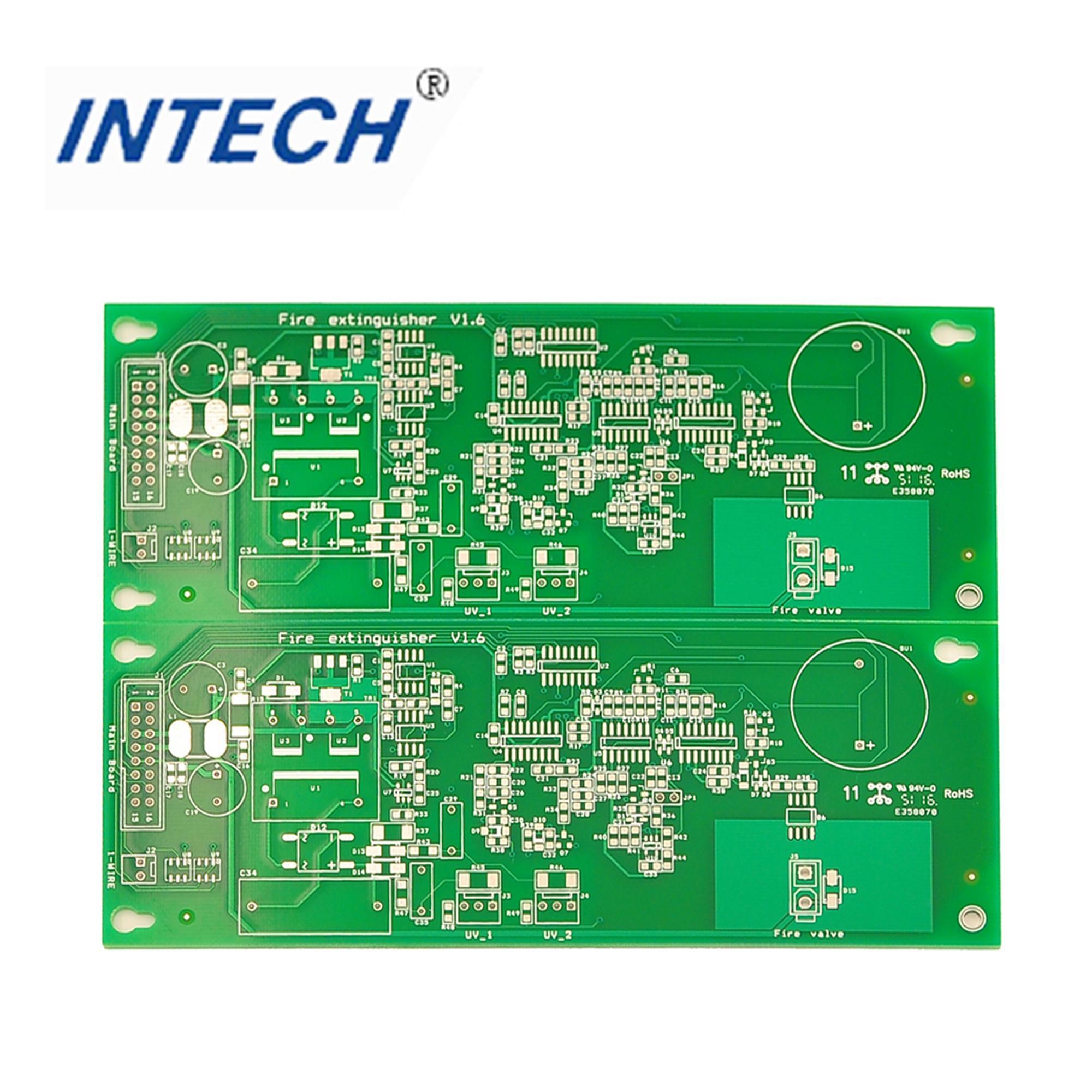
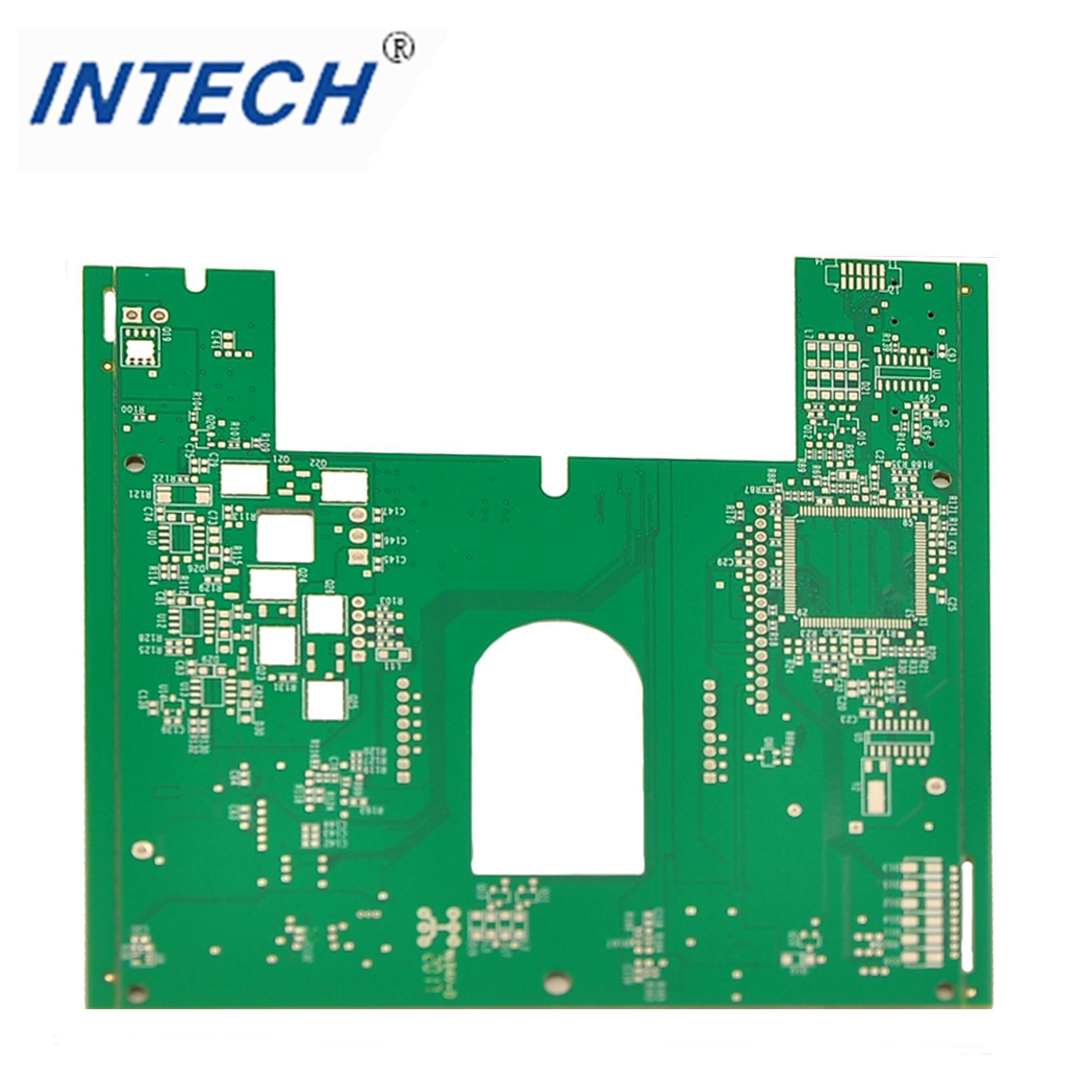
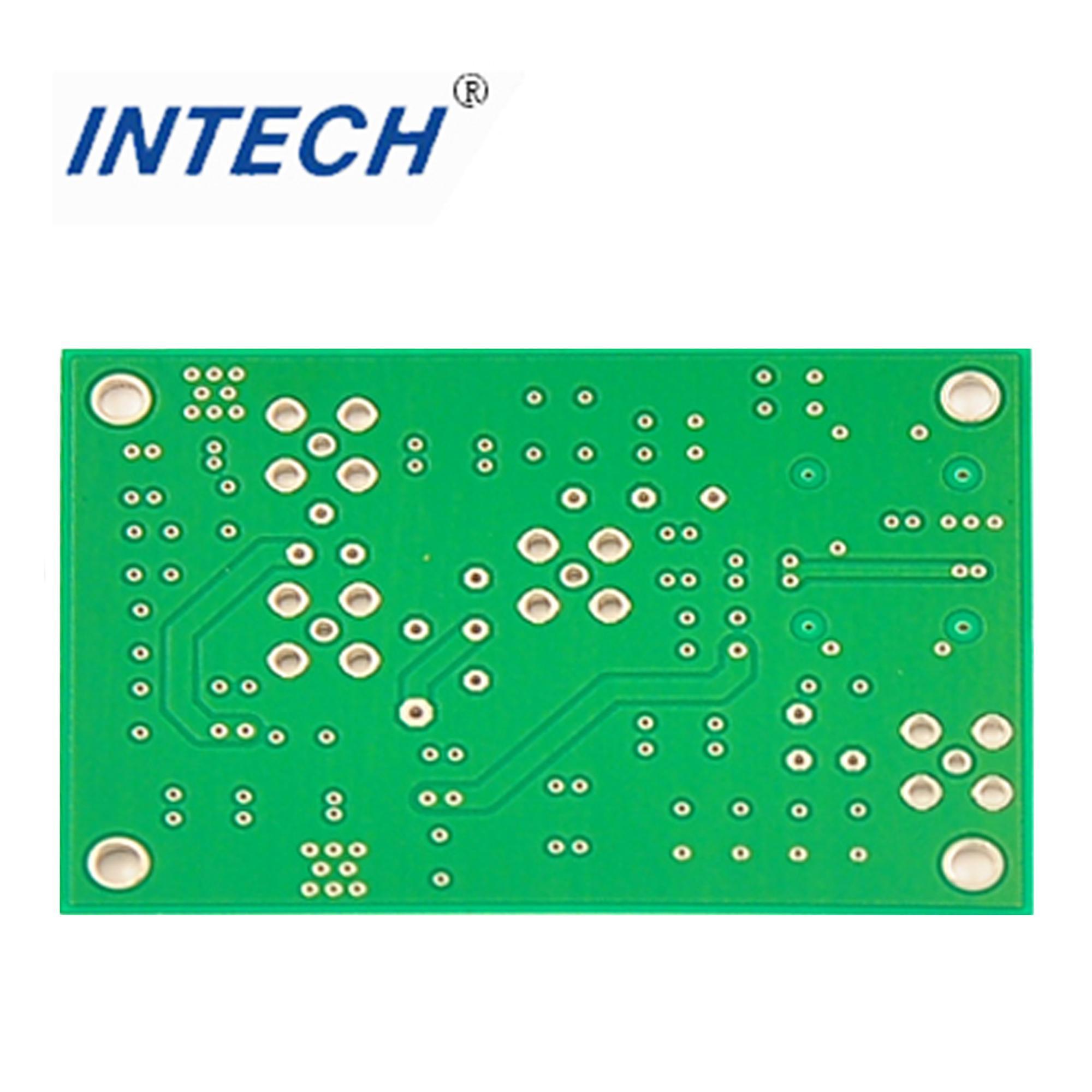
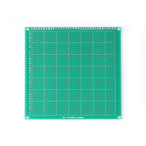
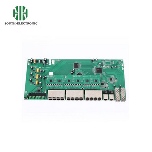
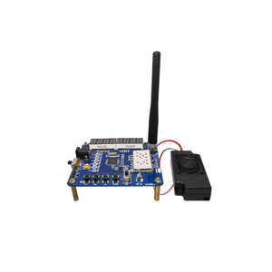
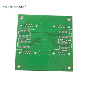
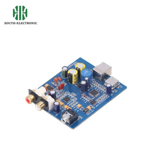
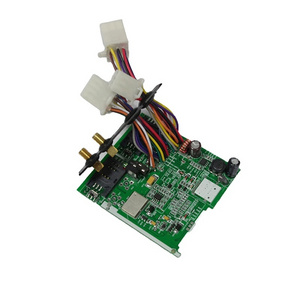
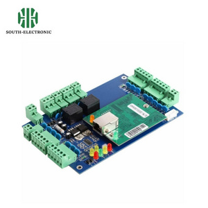
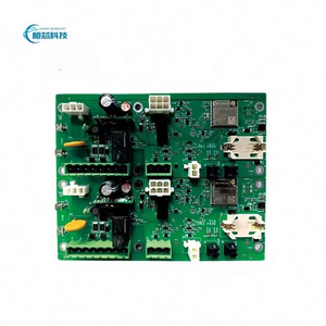
Popular new pcb design stk4050 printed circuit board in China
-
Application:
-
Consumer Electronics
-
Type:
-
Customizable
-
Certificate:
-
ISO9001/Iso14001/CE/ROHS
-
Usage:
-
OEM Electronics
-
Solder mask:
-
Green
-
Item:
-
Keyboard Pcb Assembly
-
Solder mask color:
-
Black.Red.Yellow.White.Blue.Green
-
Name:
-
PCB Board Production
-
Material:
-
FR4 CEM1 CEM3 Hight TG
Quick Details
-
Base Material:
-
FR-4
-
Board Thickness:
-
1.6mm
-
Model Number:
-
PCB
-
Place of Origin:
-
Guangdong, China
-
Brand Name:
-
PCB BOARD
-
Copper Thickness:
-
1oz
-
Min. Hole Size:
-
0.20mm
-
Min. Line Width:
-
0.1 0mm
-
Min. Line Spacing:
-
0.003"
-
Surface Finishing:
-
HASL Lead
-
Product name:
-
Popular new pcb design stk4050 printed circuit board in China
-
Application:
-
Consumer Electronics
-
Type:
-
Customizable
-
Certificate:
-
ISO9001/Iso14001/CE/ROHS
-
Usage:
-
OEM Electronics
-
Solder mask:
-
Green
-
Item:
-
Keyboard Pcb Assembly
-
Solder mask color:
-
Black.Red.Yellow.White.Blue.Green
-
Name:
-
PCB Board Production
-
Material:
-
FR4 CEM1 CEM3 Hight TG
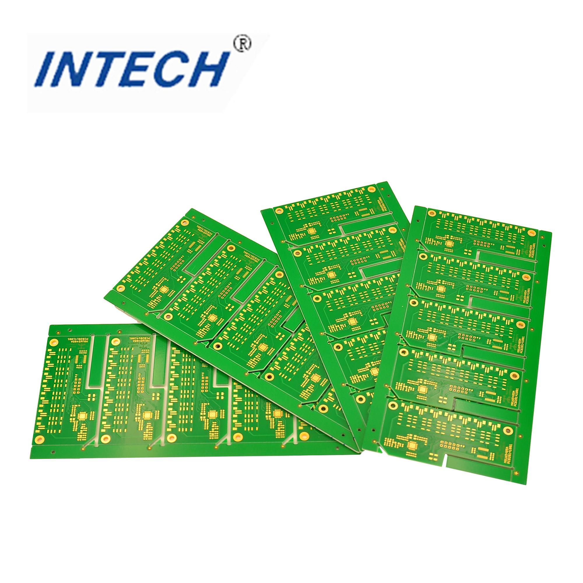
Popular new pcb design stk4050 printed circuit board in China
Product Description
| Item | Technical Parameters | Specification |
| Layers | 1-22 layers | _ |
| Min. line width | 2/2mil | Partial 2mil lines is allowed |
| Min. line space | 2/2mil | Partial 2mil lines is allowed |
| Min.annular ring width: vias | 3mil | _ |
| Min.annular ring width: component holes | 7mil | _ |
| Min.hole size(board thickness <2mm) | 4mil | _ |
| Min.hole size(board thickness ≥2mm) | Aspect ratio≤16 | _ |
| Max.board thickness(single&doule sided) | 6mm | _ |
| Max.board thickness(multilayer) | 8mm | _ |
| Min.board thickness(single&doule sided) | 0.2mm | _ |
| Min.board thickness(multilayer) | 4layers:0.4mm;6layers:0.6mm;8layers:1mm; 10layers:1.2mm | _ |
| Max.board size (single&doule sided) | 700*1200mm | _ |
| Max.board size (multilayer) | 700*1200mm | _ |
| Distance between line to board edge | Outline: 0.2mm V-CUT: 0.4mm | _ |
| Solder mask bridge | 4mil | Between IC pins |
| Solder mask color | White,black,blue,green,yellow,red,ect | _ |
| Legend color | White,black,yellow,ect | _ |
| Surface finish | HAL(with Pb free),plated Ni/Au,Immersion silver,Imm Ni/Au,Imm Sn, hard gold,OSP,ect | _ |
| Plating thickness(Technique: hard gold) | Plating type: Ni, Min./Max thickness:100/150U'' Plating type: Au, Min./Max thickness:5/120U'' | _ |
| Plating thickness (Technique:Immersion Ni/Au) | Plating type: Imm Ni, Min./Max thickness:100/150U'' Plating type: Imm Au, Min./Max thickness:2/4U'' | _ |
| Plating thickness (Technique: gold finger) | Plating type: Ni, Min./Max thickness:120/150U'' Plating type: Au, Min./Max thickness:5/120U'' | _ |
| Copper plating hole | Copper thickness: Min.20um/Max.25um | _ |
| Base copper thickness(Inner and outer layer) | Min. thickness:1/3 OZ Max.thickness:6OZ | _ |
| Finished copper thickness | Outer layers: Min.thickness 1 OZ,Max.thickness 10 OZ Inner layers: Min.thickness 0.5 OZ,Max.thickness 6 OZ | _ |
| Min.insulation layer thickness | 2mil | _ |
| Line width/space: 3/3mil,4/4mil,4/5mil | Max. Copper thickness 0.5 OZ | Line width shouldn't be less than the required value under ensure of space |
| Line width/space: 4/6mil,5/5mil,6/5mil | Max. Copper thickness 1 OZ | |
| Line width/space: 5/6mil,6/6mil | Max. Copper thickness 2 OZ | |
| Line width/space: 6/8mil,7/8mil,8/8mil | Max. Copper thickness 3 OZ | |
| Line width/space: 8/10mil,9/10mil,10/10mil | Max. Copper thickness 5 OZ | |
| Board materials | FR-4; high Tg; high CTI; halogen free; high frequency(rogers,taconic,PTFE,nelcon,ISOLA,polyclad 370 HR); thick copper | |
| Hole size tolerance | ±0.03mm | |
| Hole position tolerance | ±0.03mm | |
| Board outline tolerance | L≤100mm:0.1mm; 200mm300mm:0.4mm | |
| Finished product thickness tolerance | 0.2mm | |
| Impedance control | ± 10% | |
| Bow and twist | ≤ 0.5% | |


PCB Flow:

PCBA Flow:
Applications
More Products
Certifications
Hot Searches

