Explore More Products
- Product Details
- {{item.text}}
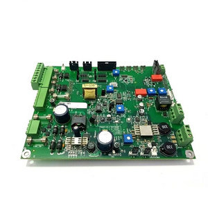
Quick Details
-
Place of Origin:
-
Guangdong, China
-
Brand Name:
-
Jinghon
-
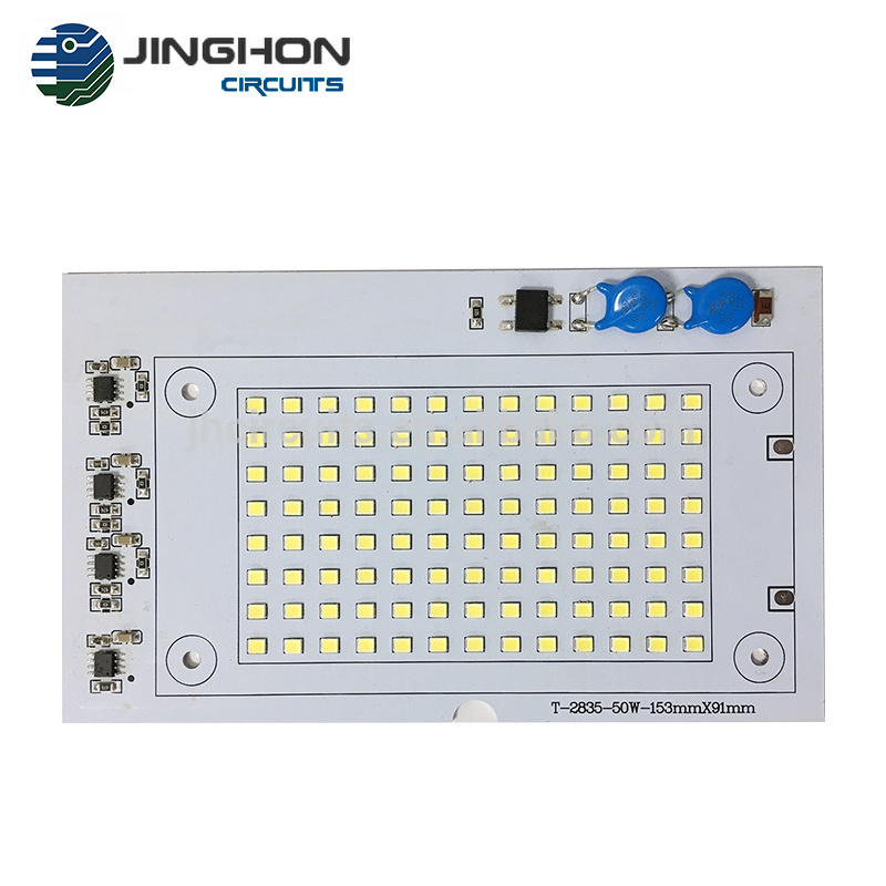
Copper Thickness:
-
1OZ
-
Min. Hole Size:
-
0.10mm
-
Min. Line Width:
-
0.10mm
-
Min. Line Spacing:
-
0.075mm
-
Surface Finishing:
-
OSP
-
Board Size:
-
OEM
-
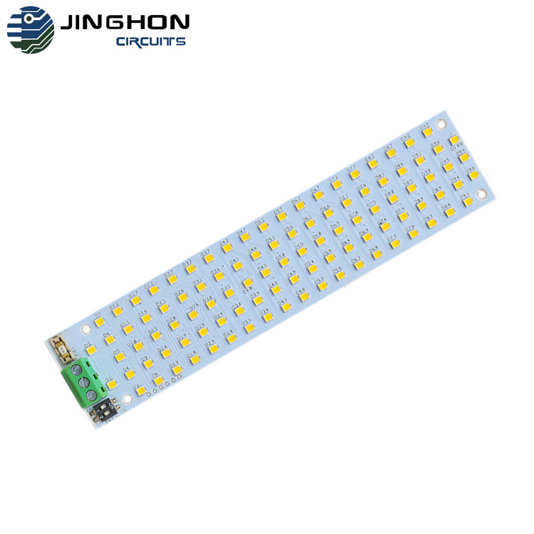
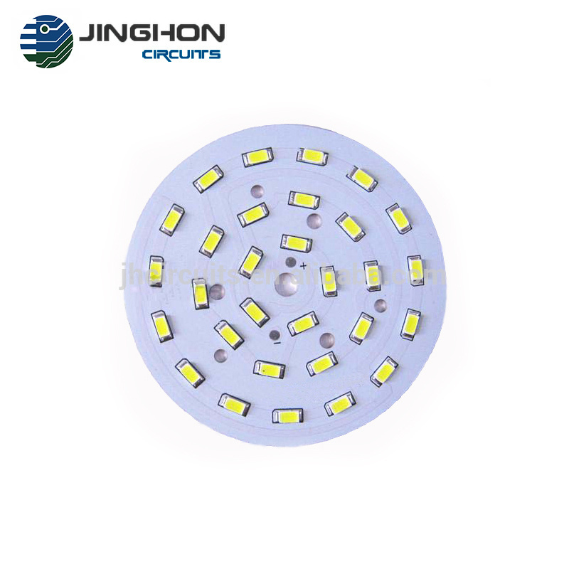
Product name:
-
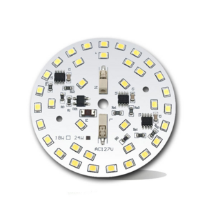
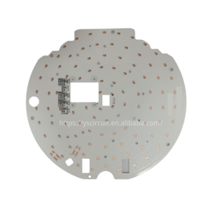
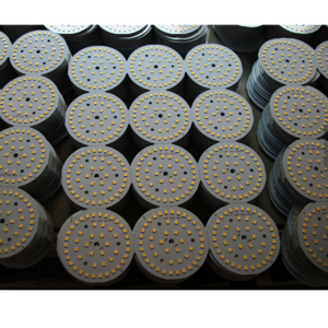
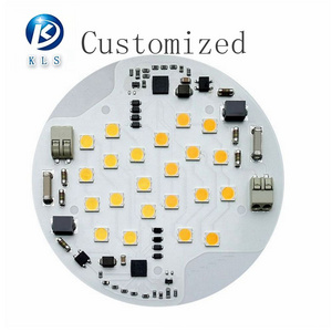
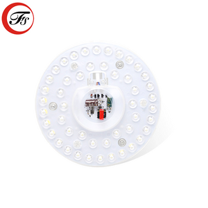
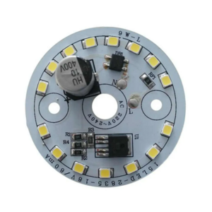
Aluminum PCB
-
Solder mask color:
-
Green Blue Black
-
Way of shipping:
-
DHL/UPS/EMS/Feldex
-
Package:
-
Vacuum package
-
MOQ:
-
1piece
-
Service:
-
EMS/OEM
-
Certification::
-
ISO9001
-
Layer Count:
-
1-24 Layer
-
Test:
-
Flying probe test /test fixture
Quick Details
-
Base Material:
-
Aluminum
-
Board Thickness:
-
2mm
-
Model Number:
-
Customized
-
Place of Origin:
-
Guangdong, China
-
Brand Name:
-
Jinghon
-
Copper Thickness:
-
1OZ
-
Min. Hole Size:
-
0.10mm
-
Min. Line Width:
-
0.10mm
-
Min. Line Spacing:
-
0.075mm
-
Surface Finishing:
-
OSP
-
Board Size:
-
OEM
-
Product name:
-
Aluminum PCB
-
Solder mask color:
-
Green Blue Black
-
Way of shipping:
-
DHL/UPS/EMS/Feldex
-
Package:
-
Vacuum package
-
MOQ:
-
1piece
-
Service:
-
EMS/OEM
-
Certification::
-
ISO9001
-
Layer Count:
-
1-24 Layer
-
Test:
-
Flying probe test /test fixture

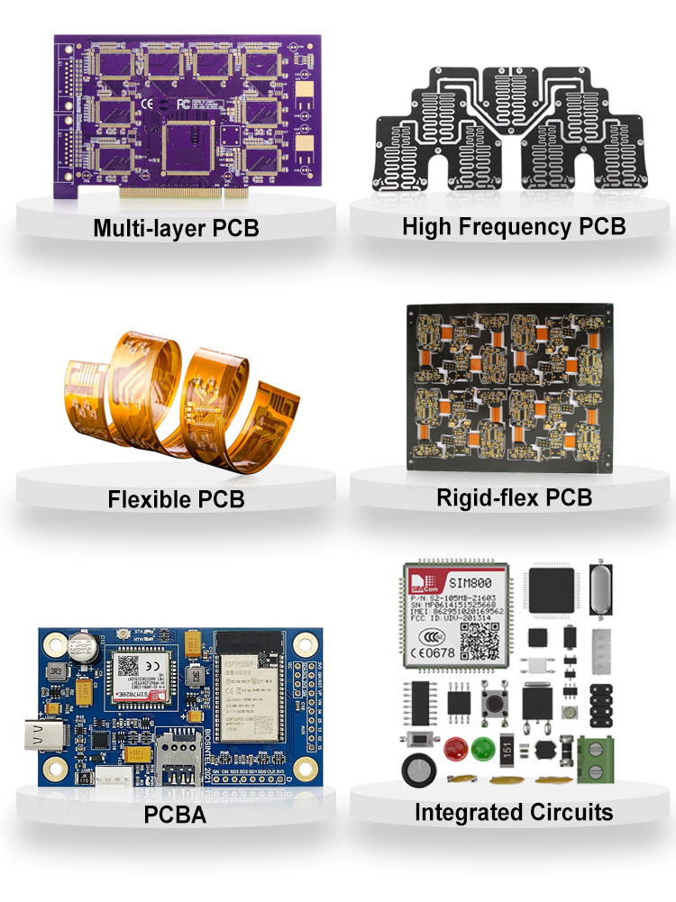
Manufacture Capacity
|
PCB Item
|
Manufacture Capacity
|
|
|
|
|
||||
|
Layer Counts
|
1--40L
|
|
|
|
|
||||
|
Base Material:
|
FR4,High-TG FR4,Halogen free,aluminum,High Frequency(Taconic,Aron,PTFE,F4B)
|
|
|
|
|
||||
|
Max board size(mm)
|
1200x400mm
|
|
|
|
|
||||
|
Board Thickness
|
0.4mm--7mm
|
|
|
|
|
||||
|
Minimum line/space
|
0.075mm
|
|
|
|
|
||||
|
Min Hole Size(mechanical)
|
0.15mm
|
|
|
|
|
||||
|
Min Hole Size(laser hole)
|
0.1mm
|
|
|
|
|
||||
|
Copper Weight
|
0.5--6oz
|
|
|
|
|
||||
|
Surface Finish
|
HAL,lead-free HAL,ENIG,Plated Gold,Immersion Gold,OSP
|
|
|
|
|
||||
|
Solder Mask
|
Green, Blue, Black, White, Yellow, Red, Matt Green, Matt Black, Matt Blue
|
|
|
|
|
||||
|
Silkscreen
|
White, Black, Blue,Yellow
|
|
|
|
|
||||
|
Acceptable File Format
|
Gerber file,Powerpcb,CAD,AUTOCAD,ORCAD,P-CAD,CAM-350,CAM2000
|
|
|
|
|
||||
|
Outline profile
|
Rout/ V-cut/ Bridge/ Stamp hole
|
|
|
|
|
||||
|
FPC Item
|
TECHNICAL PARAMETER
|
|
|
|
|
||||
|
Layers
|
1-6 Layers
|
|
|
|
|
||||
|
Mini thickness
|
0.08mm
|
|
|
|
|
||||
|
Min.Line Width
|
0.05mm
|
|
|
|
|
||||
|
Min.Hole Size
|
0.15mm PTH
|
|
|
|
|
||||
|
Min. PTH Hole Ring
|
0.45mm
|
|
|
|
|
||||
|
Min. Gap between Cover Layer and Pad
|
0.1mm
|
|
|
|
|
||||
|
Min. Gap between Trace and Outline
|
0.2mm
|
|
|
|
|
||||
|
Trace Width Tolerance
|
±0.03mm W±30%
|
|
|
|
|
||||
|
Outline Tolerance
|
±0.05mm L≤25mm
|
|
|
|
|
||||
|
Hole Size Tolerance
|
±0.05mm
|
|
|
|
|
||||
|
Stiffener and Outline Tolerance
|
±0.1mm
|
|
|
|
|
||||
|
Surface Treatment
|
ENIG,Gold Plating,HAL,Plating Pb-Sn
|
|
|
|
|
||||
|
PCBA Item
|
TECHNICAL PARAMETER
|
|
|
|
|
||||
|
Stencil size/range:
|
736x736mm
|
|
|
|
|
||||
|
Minimum IC pitch:
|
0.30mm
|
|
|
|
|
||||
|
Maximum PCB size:
|
1200x 500mm
|
|
|
|
|
||||
|
Minimum PCB thickness:
|
0.35mm
|
|
|
|
|
||||
|
Minimum chip size:
|
0201 (0.2x0.1)/0603 (0.6 x 0.3mm)
|
|
|
|
|
||||
|
Maximum BGA size:
|
74x74mm
|
|
|
|
|
||||
|
BGA ball pitch:
|
1.00mm (minimum), 3.00mm (maximum)
|
|
|
|
|
||||
|
BGA ball diameter:
|
0.40mm (minimum), 1.00mm (maximum)
|
|
|
|
|
||||
|
QFP lead pitch:
|
0.38mm (minimum), 2.54mm (maximum)
|
|
|
|
|
||||
|
Frequency of stencil cleaning:
|
1 time/5 to 10 pieces
|
|
|
|
|
||||
|
Delivery Time
|
|
|
|
|
|
|||||
|
|
Sample Lead Time
|
|
Mass Production Lead time
|
|
|
|||||
|
Single Sided PCB
|
1-2 Days
|
|
4-7 Days
|
|
|
|||||
|
Double Sided PCB
|
2-4 Days
|
|
7-10 Days
|
|
|
|||||
|
Multilayer PCB
|
5-8 Days
|
|
10-15 Days
|
|
|
|||||
|
PCB and Assembly
|
8--15 Days
|
|
15--20 Days
|
|
|
|||||
Main Products
About Us

Payment & Shipping
FAQ

Hot Searches
