Explore More Products
- Product Details
- {{item.text}}
Quick Details
-
Place of Origin:
-
Guangdong, China
-
Brand Name:
-
POE
-
Copper Thickness:
-
1oz, 1-6oz
-
Min. Hole Size:
-
0.2mm, 0.2mm
-
Min. Line Width:
-
4mil, 3.5mil
-
Min. Line Spacing:
-
4mil
-
Surface Finishing:
-
Immersion gold/hasl
-
Board Size:
-
Customized
-
Tolerance of Impedence Control:
-
5%
-
MOQ:
-
1pcs
-
PCB standard:
-
IPC-A-610 D
-
OEM/ODM:
-
One-stop Service
-
Certification:
-
ISO9001:2015, ISO13485:2016
-
Type:
-
OEM
Quick Details
-
Base Material:
-
FR4
-
Board Thickness:
-
1.6mm
-
Model Number:
-
202404251817
-
Place of Origin:
-
Guangdong, China
-
Brand Name:
-
POE
-
Copper Thickness:
-
1oz, 1-6oz
-
Min. Hole Size:
-
0.2mm, 0.2mm
-
Min. Line Width:
-
4mil, 3.5mil
-
Min. Line Spacing:
-
4mil
-
Surface Finishing:
-
Immersion gold/hasl
-
Board Size:
-
Customized
-
Tolerance of Impedence Control:
-
5%
-
MOQ:
-
1pcs
-
PCB standard:
-
IPC-A-610 D
-
OEM/ODM:
-
One-stop Service
-
Certification:
-
ISO9001:2015, ISO13485:2016
-
Type:
-
OEM
Product Description
|
item
|
value
|
|
Model Number
|
poe-03
|
|
Type
|
medical pcba
|
|
Place of Origin
|
China
|
|
|
Guangdong
|
|
Brand Name
|
POE
|
|
Supplier Type
|
factory supplier
|
|
Layers
|
1layer
|
|
Solder mask color
|
Black
|
|
Base meterial
|
FR4
|
|
Max PCB size:
|
510*460mm
|
|
Board thickness:
|
0.4-5mm
|
|
Components size
|
0201-150mm
|
|
Components Max height:
|
25mm
|
|
Min lead pitch:
|
0.3mm
|
|
Min BGA ball pitch
|
0.4mm
|
|
Placement precision:
|
+/-0.03mm
|
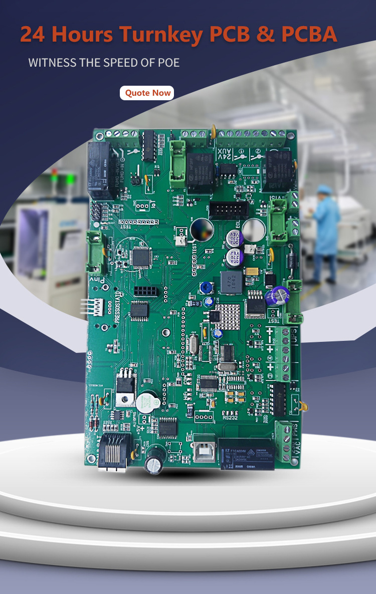


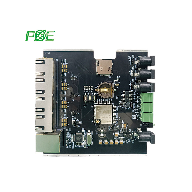
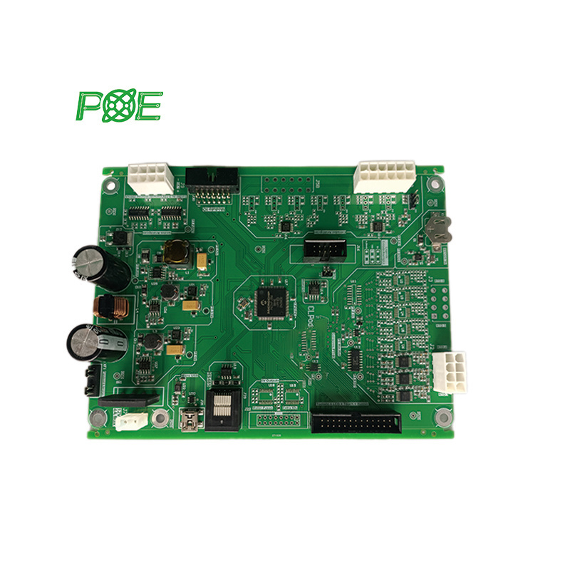
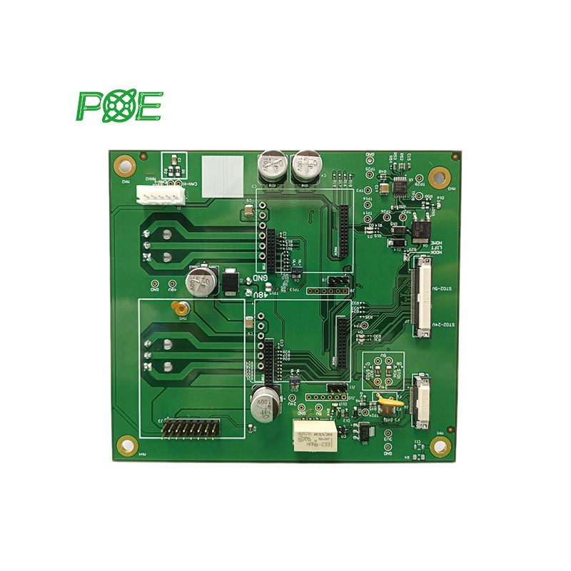
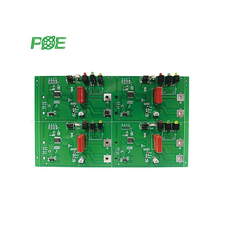
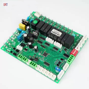
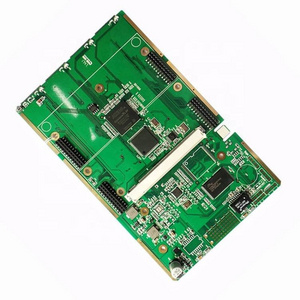
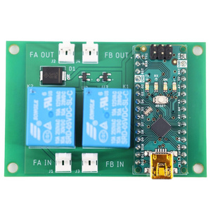
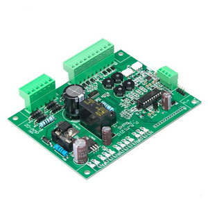
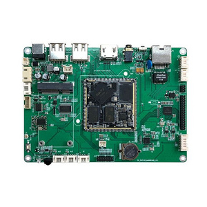
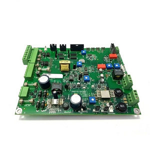
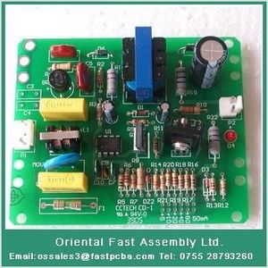
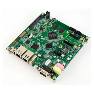
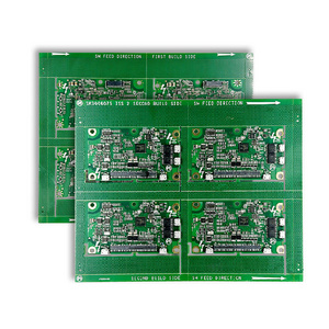
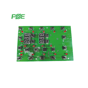
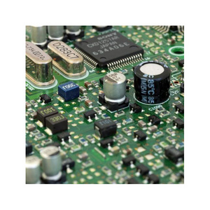
PCB Assembly Board
with SMD components
and DIP parts.
Flat and Clean DIP
parts soldering.
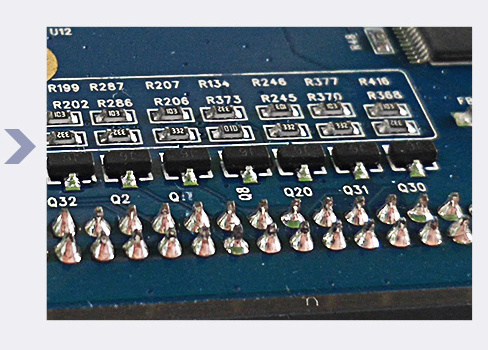
SMD Components sol-
dering from minimum
0201 package to com-
plex chips.
Application
Mainly used in the
5G, IOT, drone, smart home, telecommunications, airplane recorder, database information, home appliance,
Industrial Control, Medical Device, Automobile area LED Light, Communication,
Aviation and so on. All PCBs are ISO9001, ROHS, REACH, UL certified and meet the international IPC standard.
FAQ
Q1.What is needed for PCB PCBA quotation?
Q3. Are my files safe?
Q4. MOQ?
Q6. What service do you have?
Q7. Can we inspect quality during production?
Q8. No PCB file/Gerber file, only have the PCB sample, can you produce it for me?
Q11.What is your Lead time?
Q12. What is your testing policy and how you controle the quality?
Q13. What is your package?
PCB(printed circuit board): Quantity, Gerber file and Technic requirements(material,surface finish treatment, copper thickness,board thickness...)
PCBA(printed circuit board assembly): PCB information, BOM, (Testing documents...)
Q2. What file formats do you accept for PCB PCBA production?
Gerber file: CAM350 RS274X
PCB file: Protel 99SE, P-CAD 2001
PCB BOM: Excel (PDF, word, txt)
Q3. Are my files safe?
Your files are held in complete safety and security. We protect the intellectual property for our customers in the whole process.. All documents from customers are never shared with any third parties. We are willing to sign NDA effect by
customer side local law and promising to keep customers data in high confidential level.
customer side local law and promising to keep customers data in high confidential level.
Q4. MOQ?
There is no MOQ in POE (pcba shenzhen). We are able to handle Small as well as large volume production with flexibility.
Q5.Shipping cost?
The shipping cost is determined by the destination, weight, packing size of the goods. Please let us know if you need us to quote you the shipping cost.
Q6. What service do you have?
A: We mainly focus on PCB+ Assembly+ Components sourcing service. Additionally, we can also provide programming, testing, cables, enclosure assembly service.
Q7. Can we inspect quality during production?
Yes, we are open and transparent on each production process with nothing to hide.
We welcome customer inspect our production process and check in house.
We welcome customer inspect our production process and check in house.
Q8. No PCB file/Gerber file, only have the PCB sample, can you produce it for me?
Yes,we could help you to clone the PCB. Just send the sample PCB to us, we could clone the PCB design and work out it.
Q9. What payment do you accept ?
T/T, L/C, Western Union, Paypal, Ali Pay, Credit Cart.
Q10. Which countries have you worked with?
US, Canada, Italy, Germany, Czech Republic, Australia, Japan, and so on.
US, Canada, Italy, Germany, Czech Republic, Australia, Japan, and so on.
Q11.What is your Lead time?
Lead time is usually punctual here, usually 5-10 days for PCB sample, 10-15 days for mass production.
For some special situation, we can also advise customer in advance to avoid any inexpectation or loss at customer side.
For some special situation, we can also advise customer in advance to avoid any inexpectation or loss at customer side.
Q12. What is your testing policy and how you controle the quality?
For sample, usually tested by flying probe; for PCB Volume over 3 square meters, usually tested by fixture, this will be more faster. Due to there’s many steps to PCB production, we usually do inspection after every step.
Q13. What is your package?
With Inner vacuum package and outer carton.
Q14. PCB shipment? This is depend on customer, sometimes we ship through our forwarder, who is also the agency of DHL, TNT, UPS,
Fedex, and so on. Our forwarder can provide too much better freight cost than we get directly from those express enterprise.
Fedex, and so on. Our forwarder can provide too much better freight cost than we get directly from those express enterprise.
Hot Searches
