Products
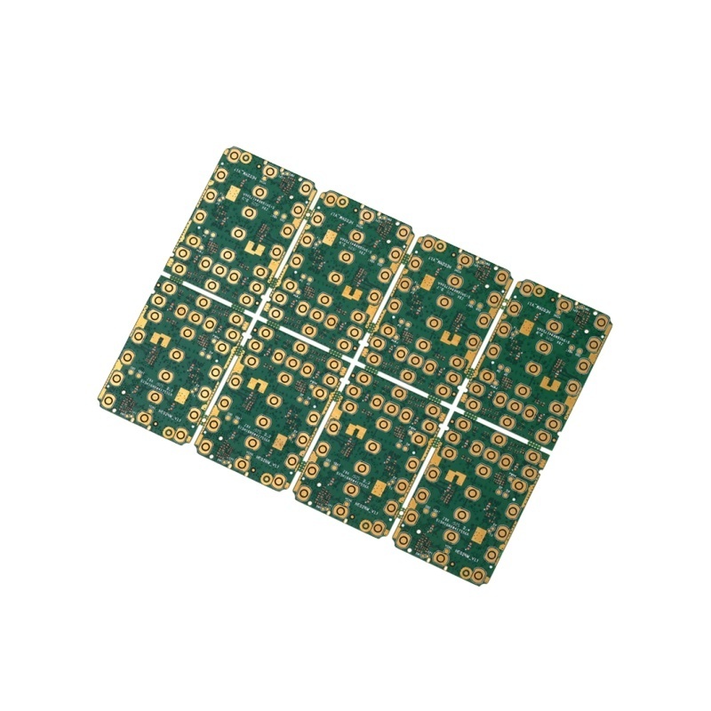
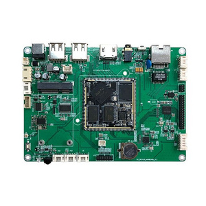
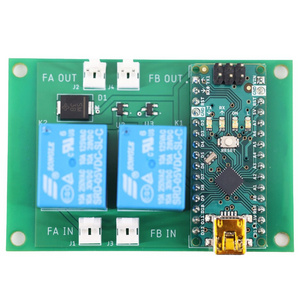
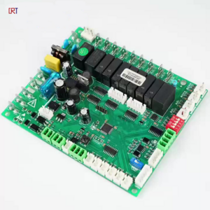
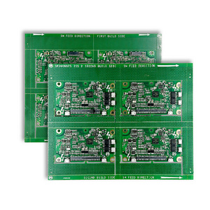
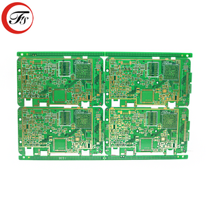
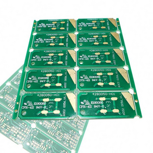
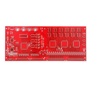
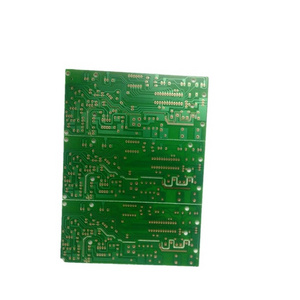
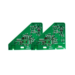
Best selling OEM custom pcb multilayer printed circuit board diy 4 layer pcb factory

Best selling OEM custom pcb multilayer printed circuit board diy 4 layer pcb factory

FOB Reference Price: Get Latest Price
≥1 Pieces
US $1.3
≥100 Pieces
US $1
≥1000 Pieces
US $0.8
Free Inquiry
Customized Request
  • Product Details
  • {{item.text}}

Quick Details

Board Size:
150*60mm
Model Number:
Semshine2024
Place of Origin:
Guangdong, China
Brand Name:
Semshine
Copper Thickness:
18um
Min. Hole Size:
0.1
Min. Line Width:
0.3
Min. Line Spacing:
0.3
Surface Finishing:
OSP
Service:
One-stop Service
SolderMask:
Green
OEM/ODM:
One-stop Quick Pcb Service
Testing Service:
Fly-probe/AOI/XRay/100%function Testing
Shipping:
Buyer's Requirement

Quick Details

Number of Layers:
4-layer
Base Material:
FR4 TG170
Board Thickness:
1.2mm
Board Size:
150*60mm
Model Number:
Semshine2024
Place of Origin:
Guangdong, China
Brand Name:
Semshine
Copper Thickness:
18um
Min. Hole Size:
0.1
Min. Line Width:
0.3
Min. Line Spacing:
0.3
Surface Finishing:
OSP
Service:
One-stop Service
SolderMask:
Green
OEM/ODM:
One-stop Quick Pcb Service
Testing Service:
Fly-probe/AOI/XRay/100%function Testing
Shipping:
Buyer's Requirement


Multilayer PCB

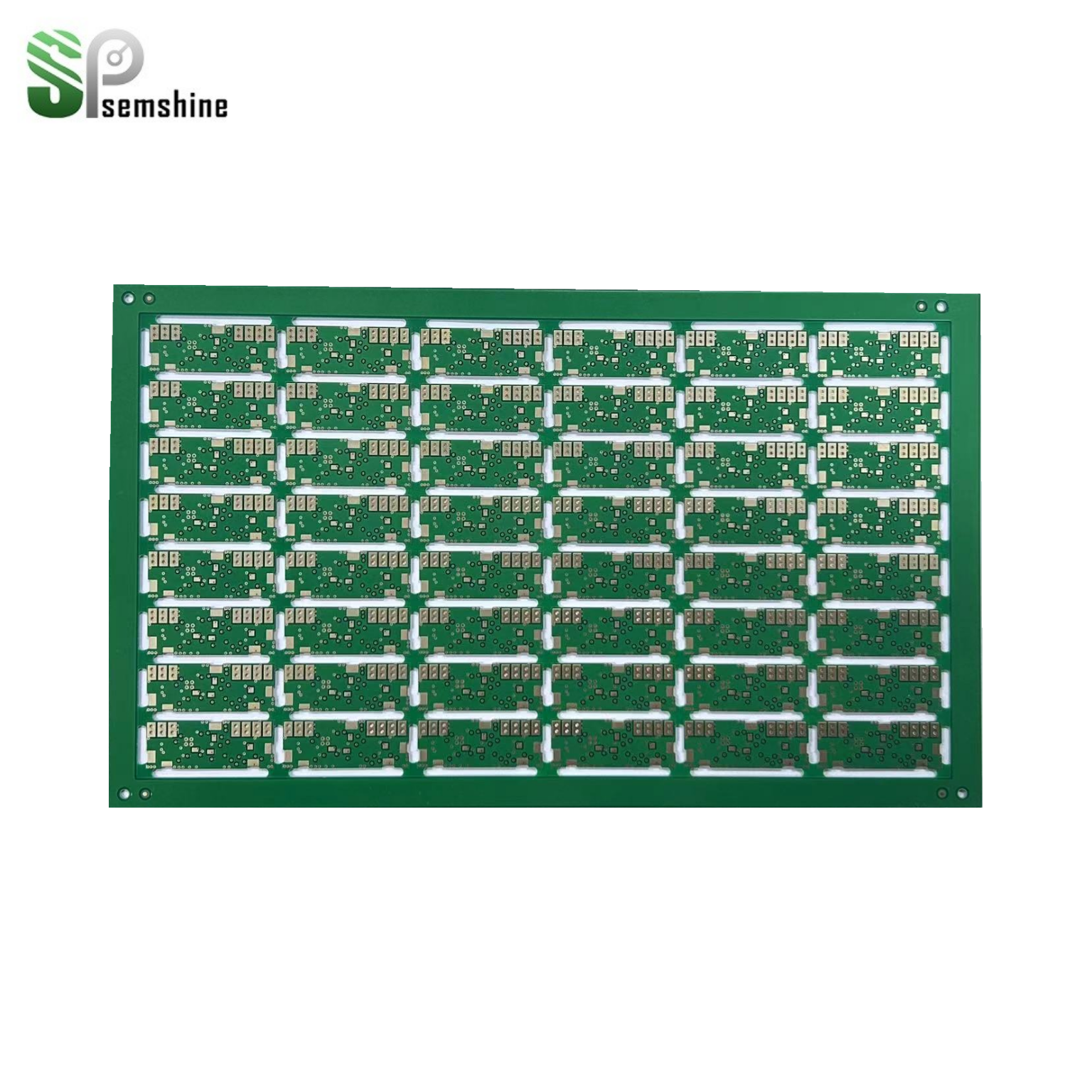
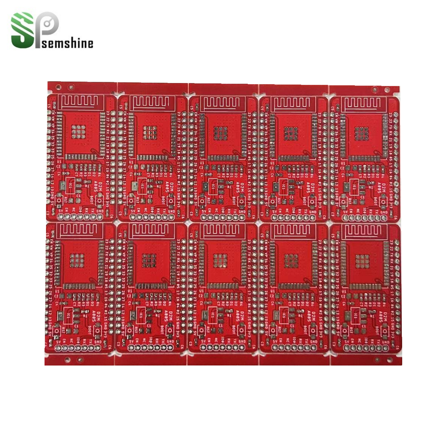
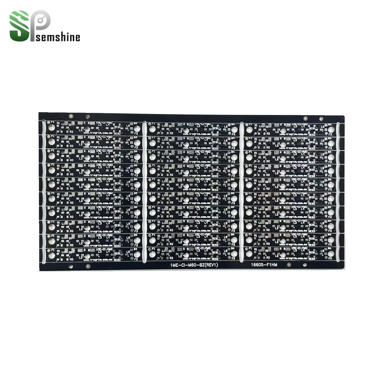
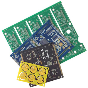
Multilayer PCB (Printed Circuit Board) refers to a type of PCB that consists of multiple layers of conductive traces and
insulating material stacked together. Unlike single-layer or double-layer PCBs, which have only one or two layers of conductive material, multilayer PCBs provide increased design flexibility and complexity by incorporating multiple layers.

In a multilayer PCB, the layers are interconnected using vias, which are small plated holes that allow electrical connections between the different layers. These vias can be through-hole vias, which traverse through all the layers, or they can be blind vias, which connect one or more inner layers but do not traverse the entire board, or buried vias, which connect inner layers without being exposed on the outer layers.

Professional Multilayer PCB manufacturer, free of Multilayer PCB proofing services,Follow-up orders schedule to ensure production time control. Multilayer PCB bulk order discount prices. Immediately consult

Category
Description
Capability


Laminate Materials
FR4(KB ILM Shengyi) High TG,Aluminumplate( Tanwan) (Single,Double-sided)
FR4 Thickness
1.6mm
High TG FR4 (170 deg c)
1.6mm

Board Cutting
Max. number of layers
16
Min.thickness for inner layers(Cu thickness are excluded)
0.07mm


Drilling
Min. size
0.1mm
Max. size
6.0mm
Drill Deviation
±0.002”(0.050mm)
PTH hole tolerance
±0.003”(0.075mm)
NPTH hole tolerance
±0.002”(0.050mm)
Angle of Countersink
80°,90 100°,120°

Drilling
Min. hole size
0.0008”
Aspect ratio
16


Etching
Trace width tolerance
±20%
Min. trace width/space (1oz finished Cu weight starting from 1/3oz)
0.003"/0.003"(0.08mm)
Min. trace width /space (1oz finished Cu weight starting from 1/2oz)
0.003"/0.004"(0.1mm)
Min. trace width / space (2oz finished Cu weight)
0.005”/0.005”(0.127mm)
Min. trace width /space (3oz finished Cu weight)
0.008"/0.008"(0.2mm)


lnner Layers
Min. space from drilling to inner pattern
0.1mm
Min. space from annular ring to inner pattern
0.1mm
Layer-to-layer registration
±0.003"(0.08mm)

Test
AOI
Y
Flying Probe Tester
Y


Controlled impedance
Tolerance
±10%
Impedance tester
Tektronix TDS8200
CNC Tolerance
±0.15mm(0.006”)
V-Cut Depth
±0.1mm(0.004")
V-cut angle deviation
±0.1mm(0.004”)
Semi-hole
Y

SEMSHINE TECH PTE,LTD is located in Singapore and was established in 2023. It relies on Shenzhen Semshine Technology Co., Ltd. Due to business development demand, we increased the Singapore branch as a sister company.

Since 2006, offers one-stop PCB manufacturing services, ranging from raw material and electronic components procurement, and PCB fabrication, to PCB assembly, testing, and after-market service.

Up to now, Semshine owns more than 20000 sqm of plant with over 60000 sqm per month production capability; and possesses the latest professional Fully automated equipment production line to handle the PCB, including double-sided, multilayer, and HDI PCBs etc. It can be widely applied to a variety of fields, such as communication, medical equipment, consumer electronics, Vehicle Electronics, etc.

With a fast delivery cycle and high -quality products, Semshine is the first choice for PCB manufacturers. And has established a good cooperative relationship with hundreds of well -known companies. We look forward to establishing a long -term cooperative relationship with you.

Why Choose Semshine

Our PCB factory
APP
Post My RFQ
WhatsApp
+86-17326049340