Explore More Products
- Product Details
- {{item.text}}
Quick Details
-
Board Size:
-
customize
-
Model Number:
-
JY PCB
-
Place of Origin:
-
Guangdong, China
-
Brand Name:
-
JY
-
Copper Thickness:
-
1~4oz
-
Min. Hole Size:
-
0.15mm
-
Min. Line Width:
-
0.08mm
-
Min. Line Spacing:
-
0.08mm
-
Surface Finishing:
-
HASL, GOLD PLATED, CARTON, OSP ,HOT AIR
-
Layer:
-
1~20 layers
-
Max. Panel Size:
-
541*647mm(Special can do to 950mm)
-
Finish Hole Size:
-
PTH +/-0.003'' ,NPTH +/-0.002"
-
Hole Position Accuracy:
-
+/-0.003"
-
Ring annulus:
-
Min 0.1mm
-
Aspect Ratio:
-
Min 1:8
-
Solder Mask Rrgistration:
-
+/-0.003"
-
Layer to layer Rrgistration:
-
+/-0.003"
-
Copper Feature to Holes Rrgistration:
-
+/-0.003"
-
Min Plated Drills to Copper:
-
0.25mm, 0.30mm
Quick Details
-
Number of Layers:
-
4-layer
-
Base Material:
-
FR4 CEM1 CEM3 Ceramic Aluminum
-
Board Thickness:
-
0.5~3.2mm
-
Board Size:
-
customize
-
Model Number:
-
JY PCB
-
Place of Origin:
-
Guangdong, China
-
Brand Name:
-
JY
-
Copper Thickness:
-
1~4oz
-
Min. Hole Size:
-
0.15mm
-
Min. Line Width:
-
0.08mm
-
Min. Line Spacing:
-
0.08mm
-
Surface Finishing:
-
HASL, GOLD PLATED, CARTON, OSP ,HOT AIR
-
Layer:
-
1~20 layers
-
Max. Panel Size:
-
541*647mm(Special can do to 950mm)
-
Finish Hole Size:
-
PTH +/-0.003'' ,NPTH +/-0.002"
-
Hole Position Accuracy:
-
+/-0.003"
-
Ring annulus:
-
Min 0.1mm
-
Aspect Ratio:
-
Min 1:8
-
Solder Mask Rrgistration:
-
+/-0.003"
-
Layer to layer Rrgistration:
-
+/-0.003"
-
Copper Feature to Holes Rrgistration:
-
+/-0.003"
-
Min Plated Drills to Copper:
-
0.25mm, 0.30mm
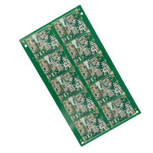
2 layer 1OZ copper leadfree HASL green solder oil mask circuit board
PCBTechnical Parameters
| No. | Item | Specification |
| 1 | PCB Layers | 1 to 24 layers |
| 2 | PCB Max working panel area | 457 x 610 mm |
| 3 | Min trace width | 0.10mm |
| 4 | Min spacing | 0.10mm |
| 5 | Min hole diameter | 0.20mm |
| 6 | Min Copper thickness in hole | 0.020mm |
| 7 | PTH size tolerance | ±0.05mm |
| 8 | NPTH size tolerance | ±0.025mm |
| 9 | Hole position tolerance | ±0.05mm |
| 10 | Dimension tolerance | ±0.1mm |
| 11 | Min solder mask dam | 0.08mm |
| 12 | Insulation resistance | 1E+12Ω (normal condition) |
| 13 | Max Board twist and wrap | ≤0.7% |
| 14 | High Vlotage endurance | 1.3KV/mm |
| 15 | Copper foil peel off endurance | 1.4N/mm |
| 16 | Hardness of resist ink | ≥6H |
| 17 | Flame resistance | 94V-0 |
| 18 | Impedance control | ±5% |
| 19 | Certificate | ISO 9001:2000;ISO 14001;ISO/TS16949:2002 , E203640 |
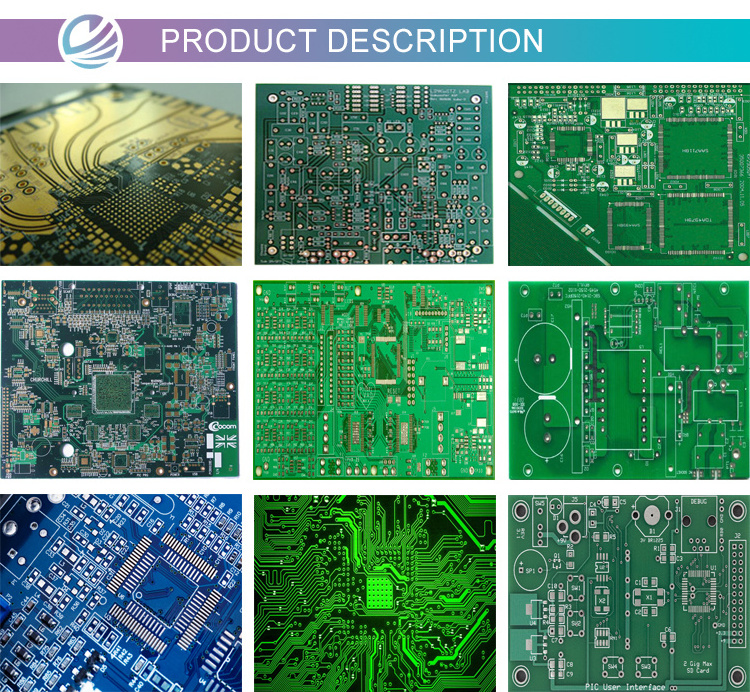
PCB Product Application Area

Circuit Board Electronic manufacturer Related Products

Our production capacity
| Technical Sepcification | What we do | What others do |
| Number of Layer | 1-32 layers(include Rigid-Flex PCB) | 1,2,4 or 6,upto 18 layer |
| Order Quantity | 60k square meter/month | 1 to 50,000 |
| Board Cutting | Shear,V-score,Tab-routed | Shear,V-score,Tab-routed |
| Board Thickness | Rigid 0.2-4.0mm, Flex 0.01-0.25mm | 0.2-4.0mm, Flex 0.01-0.25mm |
| Copper Weight | 0.2oz-10oz | 1.0, 1.5, 2.0 oz |
| Min Trace/Gap | 2mil/0.05mm | 0.10mm, or 4mils |
| Max Board Dimensions | 1000mm*600mm | 20 inch*20inch or 500mm*500mm |
| Min Drill Hole Diameter | 0.1mm | 0.01'',0.25mm, or 10mils |
| Board Thichkness Tolerance | 5-10% | ±10% |
| Copper Weight Tolerance | ± 0.15 oz | ± 0.25 oz |
| Silk Screen Min Line Width | 2mil/0.05mm | 0.006'' or 0.15mm |
| Surface Finish |
HASL,Nickle,Immersion Gold, Immersion Tin, Immersion Silver,OSP, gold plating(1-80u), tin plating, Rosin etc |
HASL,Nickle,Immersion Gold, Immersion Tin,Immersion Silver, OSP,etc |
