Explore More Products
- Product Details
- {{item.text}}
Quick Details
-
Place of Origin:
-
Guangdong, China
-
Brand Name:
-
OEM
-
Copper Thickness:
-
2oz
-
Min. Hole Size:
-
0.075mm (3mil)
-
Min. Line Width:
-
0.075mm (3mil)
-
Min. Line Spacing:
-
0.1mm (4mil)
-
Surface Finishing:
-
Gold Plating, ENIG, ImAu, HASL, OSP, etc
-
Board Size:
-
Custom size
-
Keywords:
-
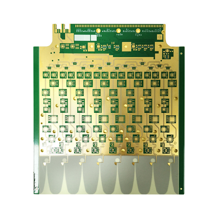
High Frequency PCB Circuit Board
-
Used for:
-
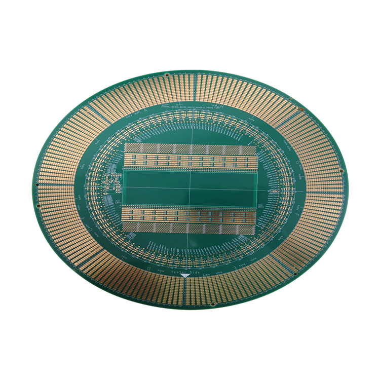
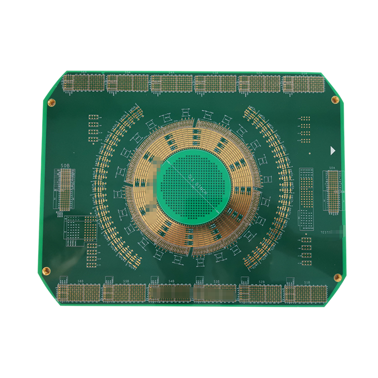
Semiconductor Testing PCB PCBA
-
Layer:
-
1-64 Layers
-
Solder Mask Color:
-
Black , Green , Blue , Red , etc
-
PCB Cutting:
-
V-Score, Tab-Routed, Counter Sunk
-
impedance control accuracy:
-
±5%
-
One stop service:
-
PCB and PCBA
-
Order Type:
-
Custom Order
-
Files we need:
-
Gerber and Bom list
-
Other materials:
-
Fr4, 94v0, F4B, RF-60, Aluminum, Polyimade,PET
Quick Details
-
Base Material:
-
Synamic 6GN
-
Board Thickness:
-
0.2-6.5mm
-
Model Number:
-
DP169
-
Place of Origin:
-
Guangdong, China
-
Brand Name:
-
OEM
-
Copper Thickness:
-
2oz
-
Min. Hole Size:
-
0.075mm (3mil)
-
Min. Line Width:
-
0.075mm (3mil)
-
Min. Line Spacing:
-
0.1mm (4mil)
-
Surface Finishing:
-
Gold Plating, ENIG, ImAu, HASL, OSP, etc
-
Board Size:
-
Custom size
-
Keywords:
-
High Frequency PCB Circuit Board
-
Used for:
-
Semiconductor Testing PCB PCBA
-
Layer:
-
1-64 Layers
-
Solder Mask Color:
-
Black , Green , Blue , Red , etc
-
PCB Cutting:
-
V-Score, Tab-Routed, Counter Sunk
-
impedance control accuracy:
-
±5%
-
One stop service:
-
PCB and PCBA
-
Order Type:
-
Custom Order
-
Files we need:
-
Gerber and Bom list
-
Other materials:
-
Fr4, 94v0, F4B, RF-60, Aluminum, Polyimade,PET

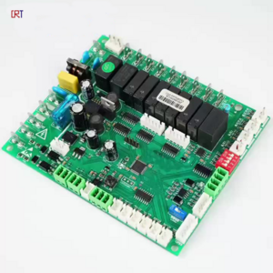
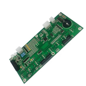
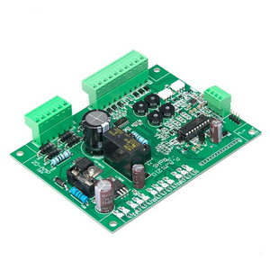
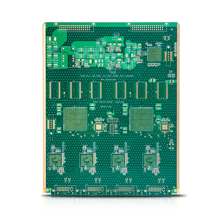
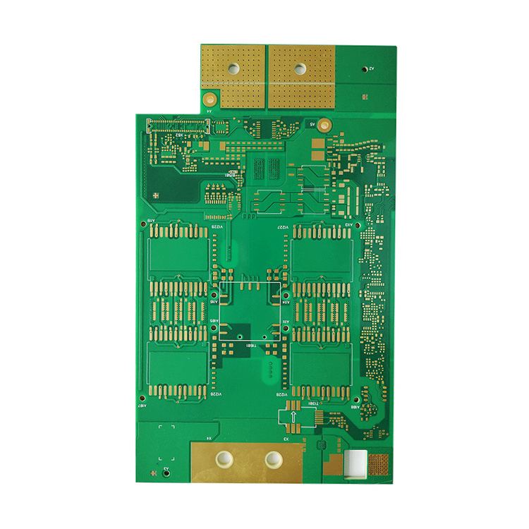
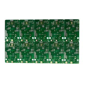
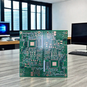
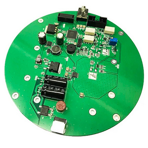
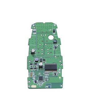
Electronic Semiconductor Testing Multilayer Printed Circuit Board High Frequency PCB PCBA Assembly Manufacturer
Our Capability
|
Order Type
|
Custom PCB and PCBA order
|
|
Application
|
Electronic Semiconductor Testing Printed Circuit Board
|
|
OEM Material
|
FR-4(High TG), Aluminum base, Polyimide, CEM-1, CEM-3, Rogers, FR4 halogen free
|
|
Max finished board size
|
610mm x 508 mm ( 24'' x 20'' )
|
|
Board thickness
|
0.2mm-6.5mm
|
|
Copper thickness
|
1oz - 5oz , always 1oz
|
|
Min. hole diameter
|
0.075mm / 3 mil with laser drilling , 0.2mm/8 mil with CNC drilling
|
|
Min. line width
|
0.75mm / 3 mil
|
|
Min. line spacing
|
0.10mm / 4 mil
|
|
Hole tolerance
|
±0.1mm
|
|
Outline tolerance
|
±0.1mm
|
|
Impedance control tolerance
|
±10%
|
|
Solder mask color
|
Double-sided Green LPI, Red, White,Blue, Black, Purple etc.
|
|
Surface treatment
|
HASL , Immersion Gold(1-3u'')/Tin/Silver , OSP , Gold plating(1-50u'')/finger , Carbon ink , Peelable mask
|
|
Certificate
|
ISO9001 , ISO14001 , SGS , UL , RoHS, IATF16949
|
Recommend Products
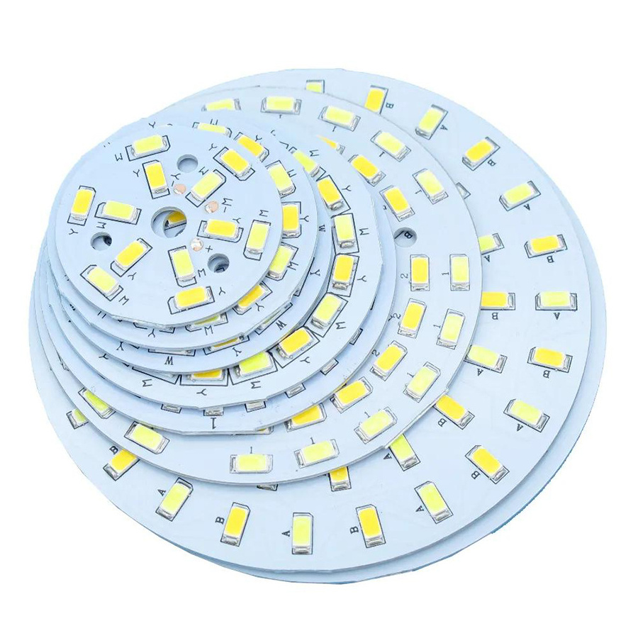
LED Aluminum PCB/PCBA High Frequency PCB Heavy Copper PCB HDI Buried via /Blind via PCB
Half-Hole PCB Rigid-Flex PCB Ultra Multilayer PCB SMT PCBA Assembly
Company Introduction
In 2011 , Diancheng Circuit was founded as a PCB manufacturer in Shenzhen . After more than 10 years , the company has developed into a one-stop service platform that provides comprehensive PCB Layout , PCB Fabrication , PCB Assembly , and Component Purchasing services .
We have passed certification of RoHS, UL, IATF16949, SGS , ISO9001, ISO14001 , REACH and others .
Now, with more than 300 technical workers and the whole production line , in each month , we can produce more than 30,000 square meters PCB and PCBA for our customers.
PCB Fabrication Workshop
Drilling Wrokshop
Circuit Transfer Workshop
AOI Workshop
Solder Mask Workshop
Routing and V-cut Workshop
ICT Testing
SMT Workshop
Solder Paste Printing
Surface Mounting
Reflow Soldering
AOI Checking
Wave Soldering
ICT Testing
Application Field
FAQ
For PCB : Quantity, Gerber file and Technic requirements(material, surface finish treatment, copper thickness, board thickness )
For PCBA : PCB information, BOM , (Testing documents)
Q2. Are my files safe?
Your files are held in complete safety and security. We protect the intellectual property for our customers in the whole
process. All documents from customers are never shared with any third parties.
Q3. MOQ?
A: There is no MOQ. We are able to handle Small as well as large volume production with flexibility.
Q4. Shipping cost?
The shipping cost is determined by the destination, weight, packing size of the goods. Please let us know if you need us to quote you the shipping cost. Q5. Can we visit your company? Yes , you will be sincerely welcomed . Q6. How long will you give us the quotation for PCB ? After we received your file , we will show you the price in 24 hours .
Hot Searches
