Products
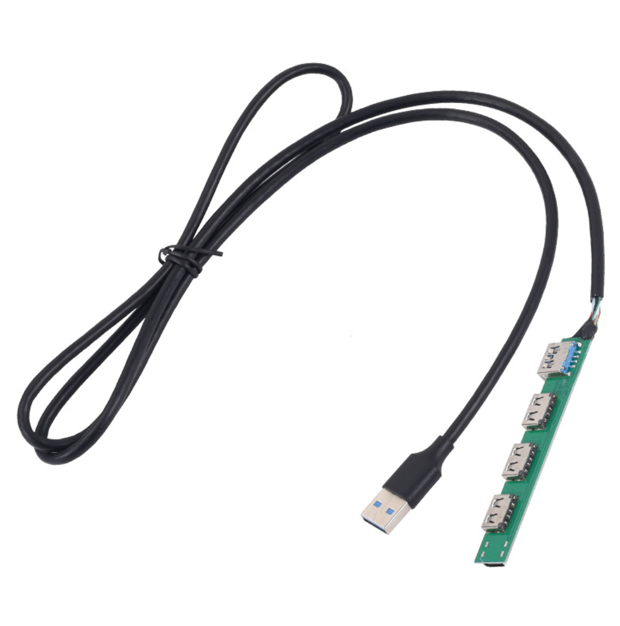
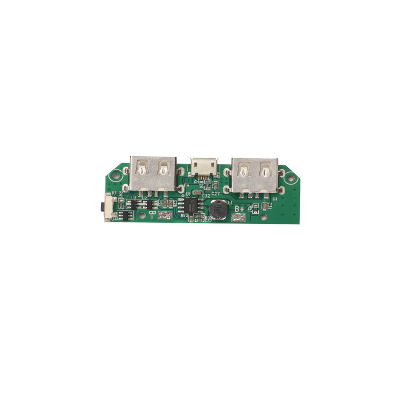
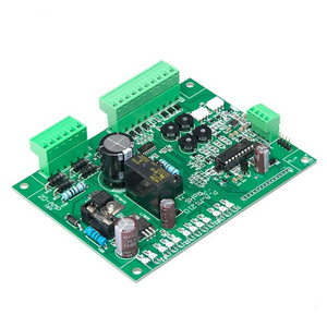
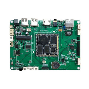
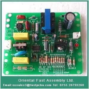
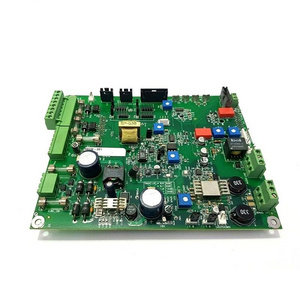
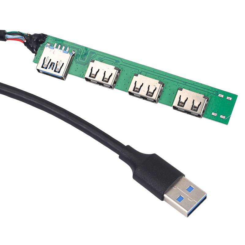
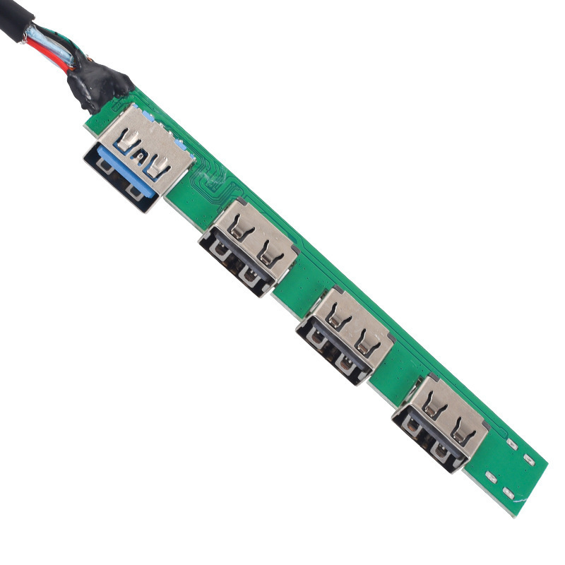
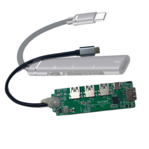
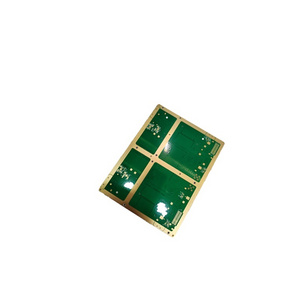
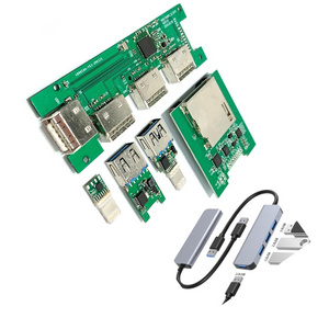
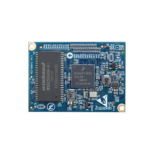
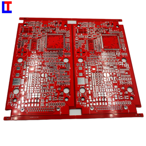
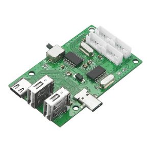
Solder USB Hub PCB  reliable electronic pcb Professional smart PCB and PCBA Type C 4 usb hub PCBA board

Solder USB Hub PCB reliable electronic pcb Professional smart PCB and PCBA Type C 4 usb hub PCBA board

FOB Reference Price: Get Latest Price
≥1 Pieces
US $2
≥1000 Pieces
US $1
Free Inquiry
Customized Request
  • Product Details
  • {{item.text}}

Quick Details

Supplier Type:
OEM/ODM
PCB type:
4 usb hub
Surface Finishing:
HASL,Lead Free HASL, OSP,ENIG,Gold plating
Material:
FR4,FR1,CEM3,Aluminum,Ceramic
Color:
Customized Color
Testing Service:
AOI X-Ray Function Test
Certificate:
ISO9001/Iso14001/CE/ROHS
MOQ:
1 PCS
PCBA service:
SMD SMT DIP Component Assembly
Item:
Custom Circuit Board

Quick Details

Model Number:
KW090A
Place of Origin:
Shenzhen
Brand Name:
Kewei
Supplier Type:
OEM/ODM
PCB type:
4 usb hub
Surface Finishing:
HASL,Lead Free HASL, OSP,ENIG,Gold plating
Material:
FR4,FR1,CEM3,Aluminum,Ceramic
Color:
Customized Color
Testing Service:
AOI X-Ray Function Test
Certificate:
ISO9001/Iso14001/CE/ROHS
MOQ:
1 PCS
PCBA service:
SMD SMT DIP Component Assembly
Item:
Custom Circuit Board
Product Description
PCB capability(can customize with complete line )
Layer count
1-18 layers
Material
fr4,Tg=135,150,170,180,210,cem-3,cem-1,al base,rogers,nelco
Copper thickness
1/2oz,1oz,2oz,3oz,4oz,5oz
Board thickness
8-236mil(0.2-6.0mm)
Min.line width/space
3/3 mil(75/75um)
Min. drill size
8 mil(0.2mm)
Min. HDI laser drill size
3 mil(0.067mm)
Tolerance of hole size
2 mil(0.05mm)
PTH copper thickness
1 mil(25 um)
Solder mask color

Customized
Peelable solder mask
Yes
surface treating
HASL(ROHS), ENING,OSP,IMMERSION SILVER,IMMERSION TIN,flash gold
Gold thickness
2-30u" (0.05-0.76um)
Blind hole/buried hole
Yes
V-cut
Yes
PCBA capability
Technology
SMT, THT
SMT capability
4,000,000 points per day
DIP capability
600,000 points per day
Experiences
QFP, BGA, μBGA, CBGA
Process
Lead-free
Programming
Yes
Conformal coating
Yes
PCBA (PCB Assembly)
-IQC
-automatic solder paste printing
-SPI
-SMT
Reflow soldering
-AOI
-X-RAY (for BGA)
-ICT testing
-DIP through hole
-Wave soldering
-Board cleaning
-Firware Programming
-Fuction Testing
Finished Product
-PCB assembly with wires & cable Assembly
-PCB assembly with plastic cases
-PCB assembly with metal enclosures

All products are 100% tested and QCed before Shipment
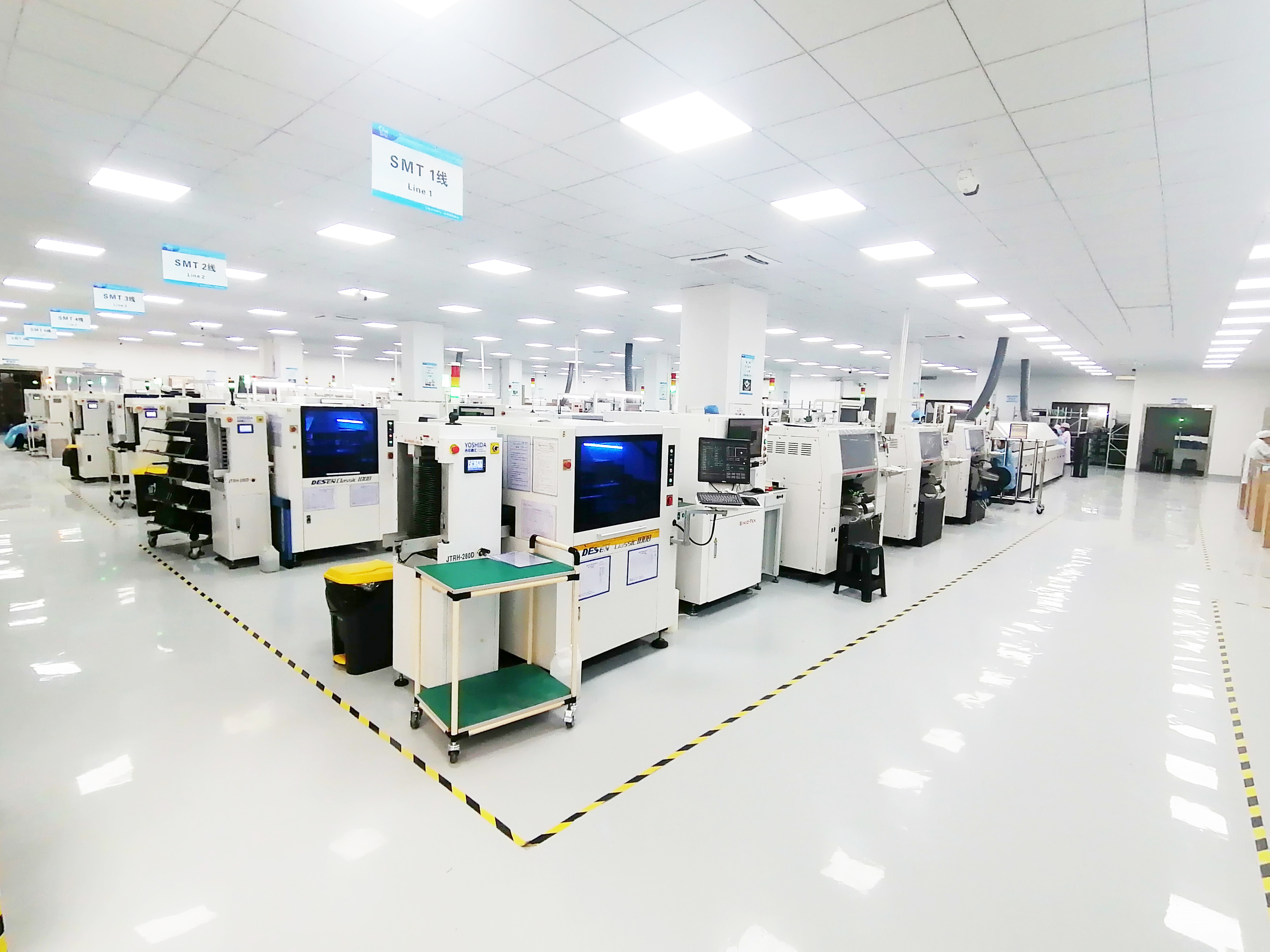
SMT Manufacturing
SMT Manufacturing Capability
Item
Manufacturing Capability & Method
Production size(Min/Max)
50×50mm / 500×500mm
Production board thickness
0.2 ~ 4mm


Printing solder paste
Support method
Magnetism fixture, vacuo platform
Clamping method
Sticking up by vacuo, clamping on both sides ,flexible clamping with sheet, flexible clamping with thick board
Cleaning Method of printing solder paste
Dry method+ wetting method+ Vacuo method
Accuracy of printing
±0.025mm
SPI
Repeated accuracy of volume
<1% at 3σ


Mounting component
Components size
0603(Option) L75mm Connector
Pitch
0.15mm
Repeated accuracy
±0.01mm

AOI
FOV size
61×45mm
Test speed
9150mm²/Sec
3D X-ray
Shootingangle
0-45
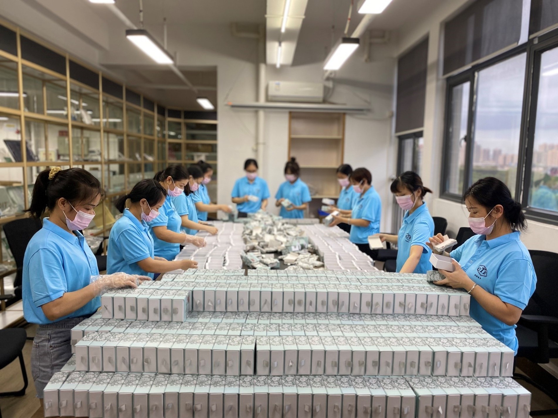
Packing&Shipping
Shipping
Customer Photos
Our Team

FAQ

Q1:Are you a factory or trade company?
A: We are the factory, we have our own PCB manufacturing & Assembly factory.

Q2:What kind of PCB file format can you accept for production?
A:Gerber, PROTEL 99SE, PROTEL DXP, POWER PCB, CAM350, GCCAM, ODB+(.TGZ)

Q3:Are my PCB files safe when I submit them to you for manufacturing?
A:We respect customer's copyright and will never manufacture PCB for someone else with your files unless we receive written.Permission from you, nor we'll share these files with any other 3rd parties. We can sign NDA file if you need.

Q4:No PCB file/Gbr file, only have the PCB sample,can you produce it for me?
A: Yes,we could help you to clone the PCB. Just send the sample PCB to us, we could clone the PCB design and work out it.

Q5:What is Chuante lead time?
A :Sample:
-2 Layers: 5 to 7working days
4-8 Layers: 12 working days
Mass production:
1-2 Layers:7 to 15 working days
4-8 Layers:10 to 18 working days
The leadtime is depends on your final confirmed quantity.

Q6:What payment do you accept ?
A:-Wire Transfer(T/T)-Western Union-Letter of Credit(L/C)-Paypal-Ali Pay-Credit Cart

Q7:How to get the PCBs?
A:For small packages, we will ship the boards to you by DHL,UPS,FedEx,EMS. Door to door service!
You will get your PCBs at yourhome.For heavy goods more than 300kg, we may ship your PC boards by ship or by air to save freight cost. Of course, if you have yourown forwarder, we may contact
them for dealing with your shipment.

Q8:What is your minimum order quantity?
A: No MOQ.Q9:How about your factory production
capacity?A:we can provide 100000 square meter/month.Q10:Which countries have you worked with?A:US, Canada, Italy, Germany, Czech
Republic, Australia, Japan, and so on.
APP
Post My RFQ
WhatsApp
+86-17326049340