
Explore More Products
- Product Details
- {{item.text}}
Quick Details
-
Model Number:
-
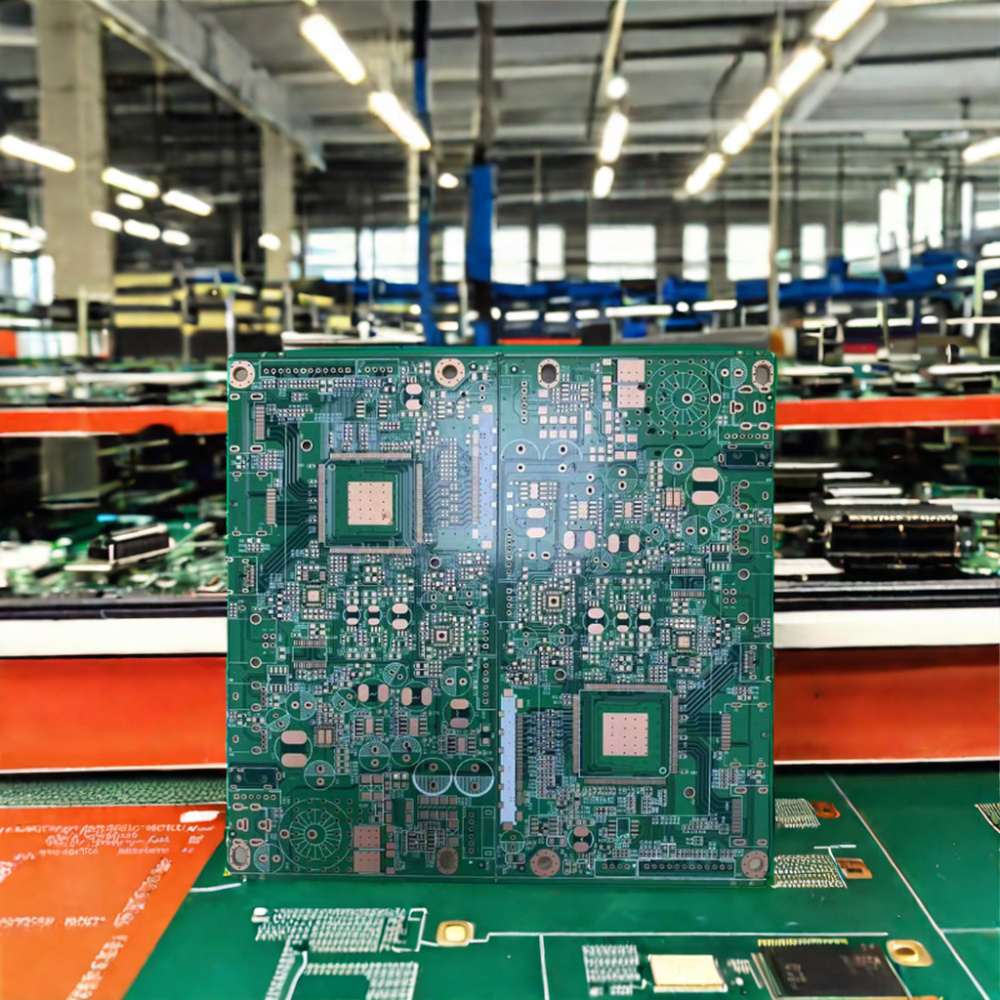
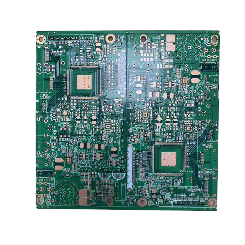
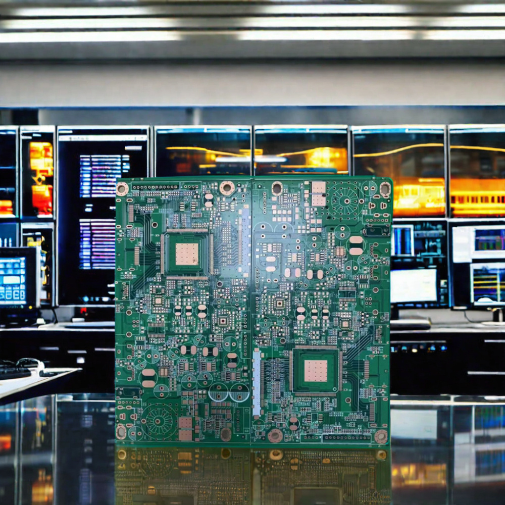
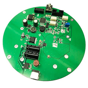
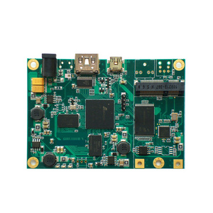
Multilayered PCB
-
Place of Origin:
-
Sichuan, China
-
Brand Name:
-
OEM
-
Copper Thickness:
-
1OZ, 1OZ
-
Min. Hole Size:
-
0.2mm
-
Min. Line Width:
-
0.1mm
-
Min. Line Spacing:
-
0.1mm
-
Surface Finishing:
-
HASL, Enig, OSP, Gold Finger
-
Material:
-
FR4
-
Surface treatment:
-
Lead-free HASL/ENIG/OSP
-
Layer Number:
-
4Layer
-
Shape:
-
Customized
-
PCB size:
-
Support Customization
-
Test Service:
-
Flying Probe Testing
-
PCB Standard:
-
IPC-II Standard
-
Solder mask color:
-
Green.Black.Red.Yellow.White.Blue.Purple.Matte Green. Matte Black
-
PCB:
-
Multilayer Pcb Packaging
Quick Details
-
Number of Layers:
-
4-layer
-
Base Material:
-
FR4
-
Board Thickness:
-
1.6-4.5mm
-
Model Number:
-
Multilayered PCB
-
Place of Origin:
-
Sichuan, China
-
Brand Name:
-
OEM
-
Copper Thickness:
-
1OZ, 1OZ
-
Min. Hole Size:
-
0.2mm
-
Min. Line Width:
-
0.1mm
-
Min. Line Spacing:
-
0.1mm
-
Surface Finishing:
-
HASL, Enig, OSP, Gold Finger
-
Material:
-
FR4
-
Surface treatment:
-
Lead-free HASL/ENIG/OSP
-
Layer Number:
-
4Layer
-
Shape:
-
Customized
-
PCB size:
-
Support Customization
-
Test Service:
-
Flying Probe Testing
-
PCB Standard:
-
IPC-II Standard
-
Solder mask color:
-
Green.Black.Red.Yellow.White.Blue.Purple.Matte Green. Matte Black
-
PCB:
-
Multilayer Pcb Packaging
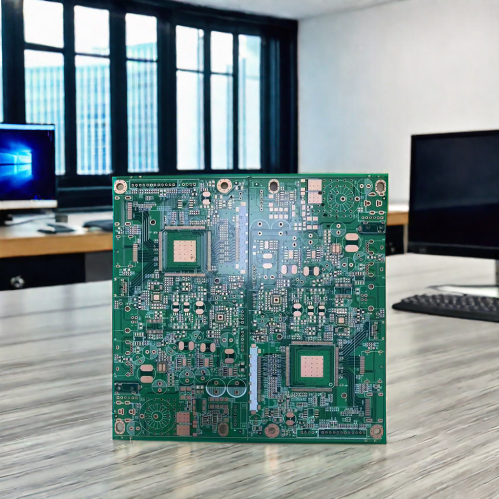
Double Sided PCB
|
SQ
|
ITEM
|
CAPABILITY
|
|
1
|
Base Material
|
FR-4, High TG FR-4 ,CEM-3,CEM-1,PTFE,Rogers ,Arlon,Taconic,X,PI ,etc
|
|
2
|
Layers
|
1-4 layers
|
|
3
|
Finished copper thickness
|
0.5-4.5 OZ
|
|
4
|
Finished Board thickness
|
0.4-2.2mm,≤0.4mm for HASL
|
|
5
|
Max b oard size
|
≤2sidesPCB: 600*1500mm Multilayer PCB: 500*1200mm
|
|
6
|
Min conductor line width
|
Inner layers:≥3/3mil Outer layers: 23.5/3.5mil
|
|
7
|
Min hole size
|
Mechanical hole: 0. 15mm Laser hole: 0.1mm
|
|
8
|
Controlled Impedance
|
+/- 5 % 2(<502).+/-10%(2500),.>5002+/-5% (needs review)
|
|
9
|
Aspect Ratio
|
15:01
|
|
10
|
Min welding ring
|
4mil
|
|
11
|
Min solder mask bridge
|
≥0.08mm
|
|
12
|
Plugging vias capability
|
0.15-0. 8mm
|
|
13
|
Hole tolerance
|
PTH: +/-3mil NPTH: +/-2mil
|
|
14
|
Outine profile
|
Rout/ V-cut/ Bridge/ Stamp hole
|
|
15
|
Solder mask color
|
Green,yellow,black,blue,red,white,matte green
|
|
16
|
Component mark color
|
white,yellow,black
|
|
17
|
Surface treatment
|
OSP/ HASL/Lead free HASL/ENIG/ENEPIG/ Au /Immersion Tin/ Immersion
Silver/Gold plating
|
|
18
|
E-Test
|
Flying probe tester: 0.4-6.0mm,max 19.6*23. 5inch
|
|
|
|
Min spacing from test pad to board edge : 0.5 mm
|
|
|
|
Min conductive resistance :5 Q
|
|
|
|
Max insulation resistance : 250 MQ
|
|
|
|
Max test voltage : 500 V
|
|
|
|
Min test pad diameter:6 mil
|
|
|
|
Min test pad to pad spacing: 10 mil
|

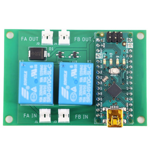
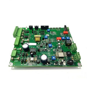
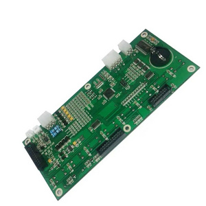
Applicable to a wide range of high-tech industries such as: telecommunications, power supply, computer, industrial control,digital products, scientific and educational instruments, medical equipment, automobiles, aerospace defense and so on.
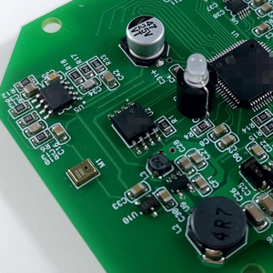
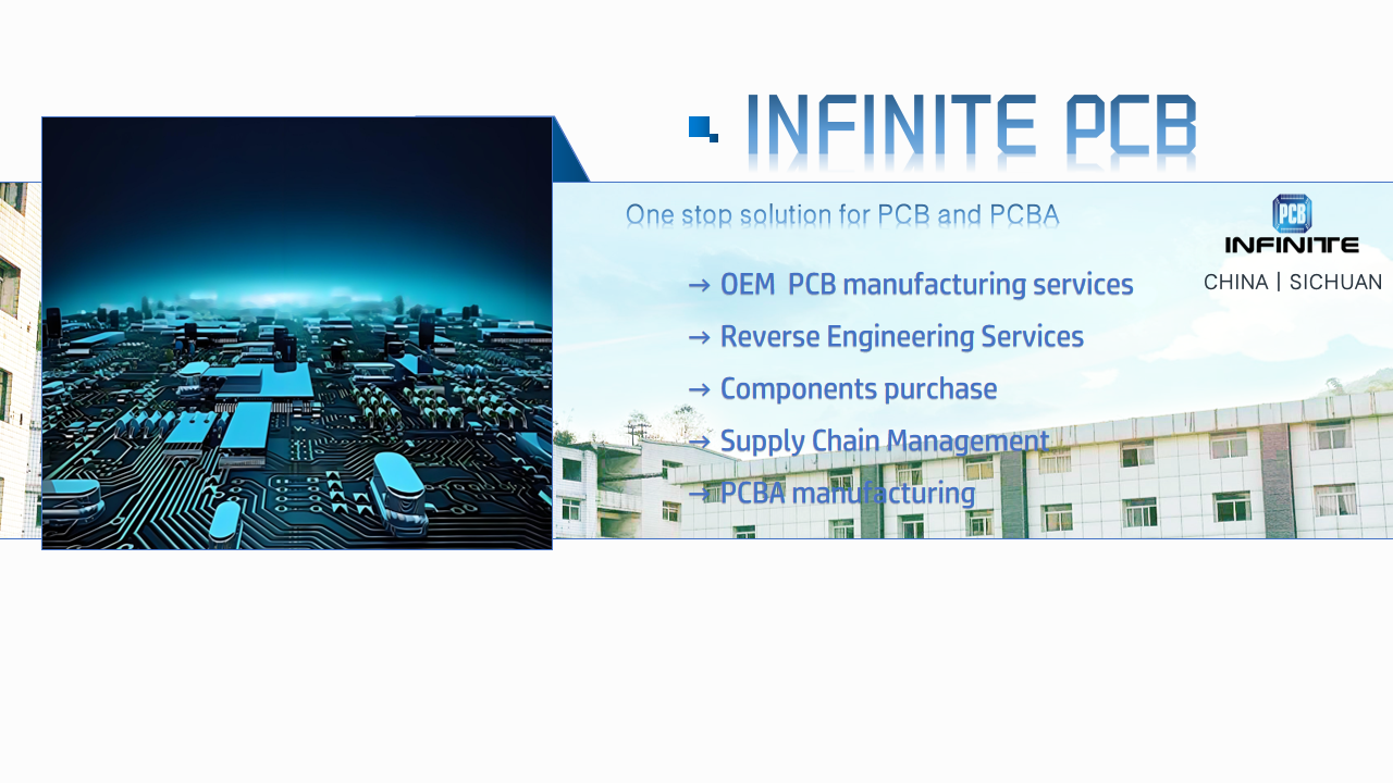
Infinite PCB is a professional company specializing in the research, development, sales, and service of PCB and PCBA.
Our affiliated factory offers a one-stop contract manufacturing solution for global customers, including PCB manufacturing, PCB assembly, component sourcing, program testing, and final packaging.
Our Services & Strength
*Trusted on time delivery
*Qualified engineering professionals
*Extremely competitive pricing
*Dedicated sales representatives for fast response times
*15 years experience
*BOM sourcing service
*A full set of production equipment
Hot Searches
