Explore More Products
- Product Details
- {{item.text}}
Quick Details
-
Material:
-
FR4 Circuit Board
-
Board Thickness:
-
1.5-1.6mm
-
Service type:
-
OEM/ODM
-
Soldermask Color:
-
Green/ White/ Black/ Blue/ Yellow
-
Layer:
-
1-24 Layers
-
Testing Service:
-
Fly-probe,100% AOI testing, 100% ET testing,
-
Keywords:
-
PCBA
-
Surface Finishing:
-
HASL,OSP,ENIG, Gold finger
-
Min. Hole Size:
-
0.2mm
-
PCB Standard:
-
IPC-II Standard
Quick Details
-
Model Number:
-
FR407
-
Place of Origin:
-
Guangdong, China
-
Supplier Type:
-
OEM
-
Material:
-
FR4 Circuit Board
-
Board Thickness:
-
1.5-1.6mm
-
Service type:
-
OEM/ODM
-
Soldermask Color:
-
Green/ White/ Black/ Blue/ Yellow
-
Layer:
-
1-24 Layers
-
Testing Service:
-
Fly-probe,100% AOI testing, 100% ET testing,
-
Keywords:
-
PCBA
-
Surface Finishing:
-
HASL,OSP,ENIG, Gold finger
-
Min. Hole Size:
-
0.2mm
-
PCB Standard:
-
IPC-II Standard
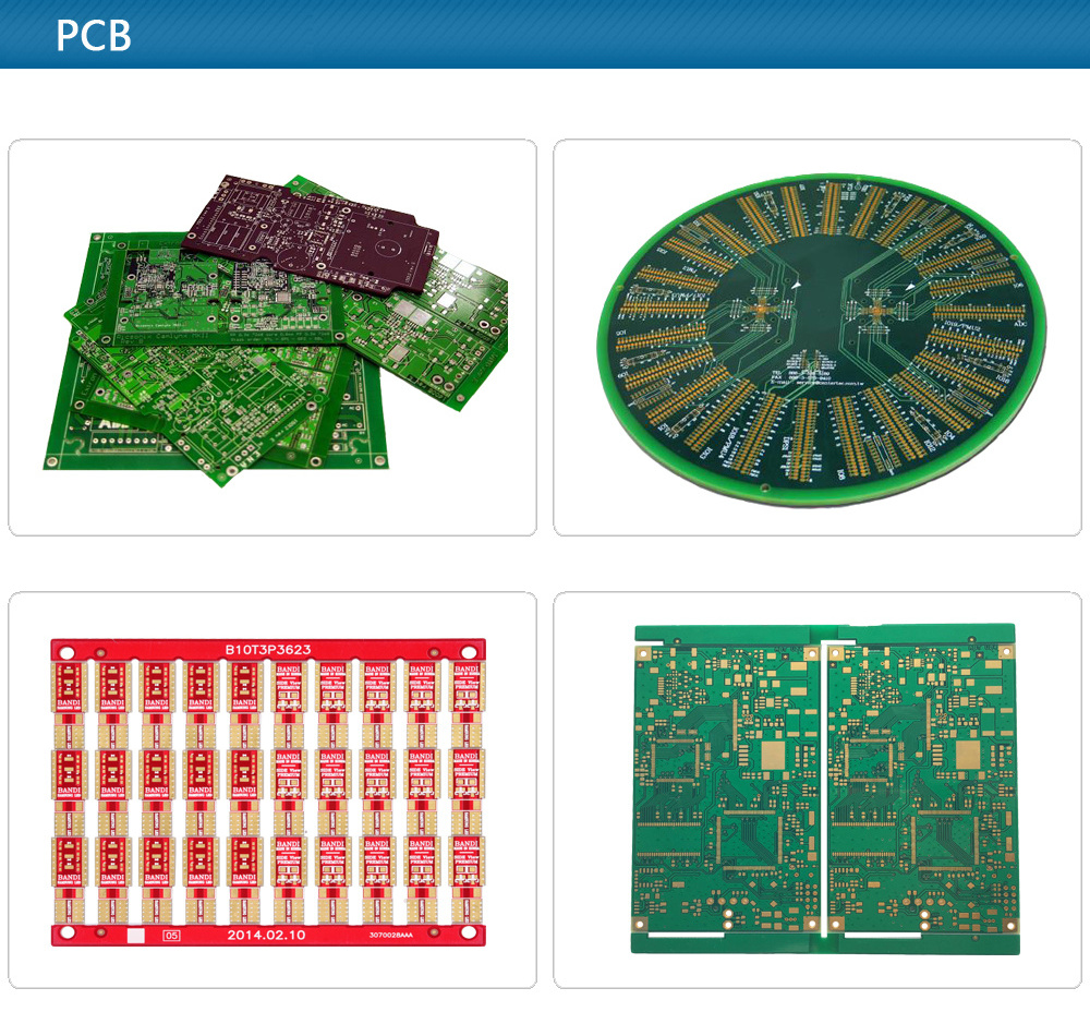
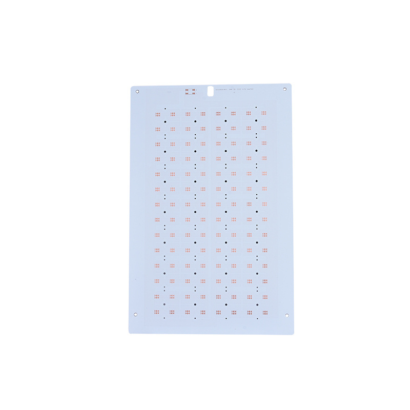
Products Description
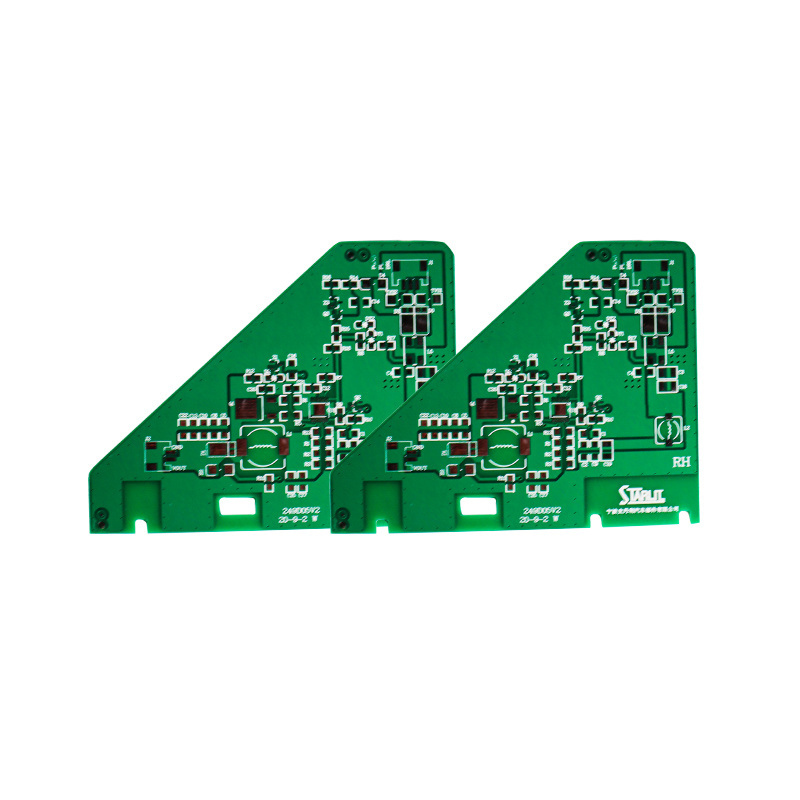
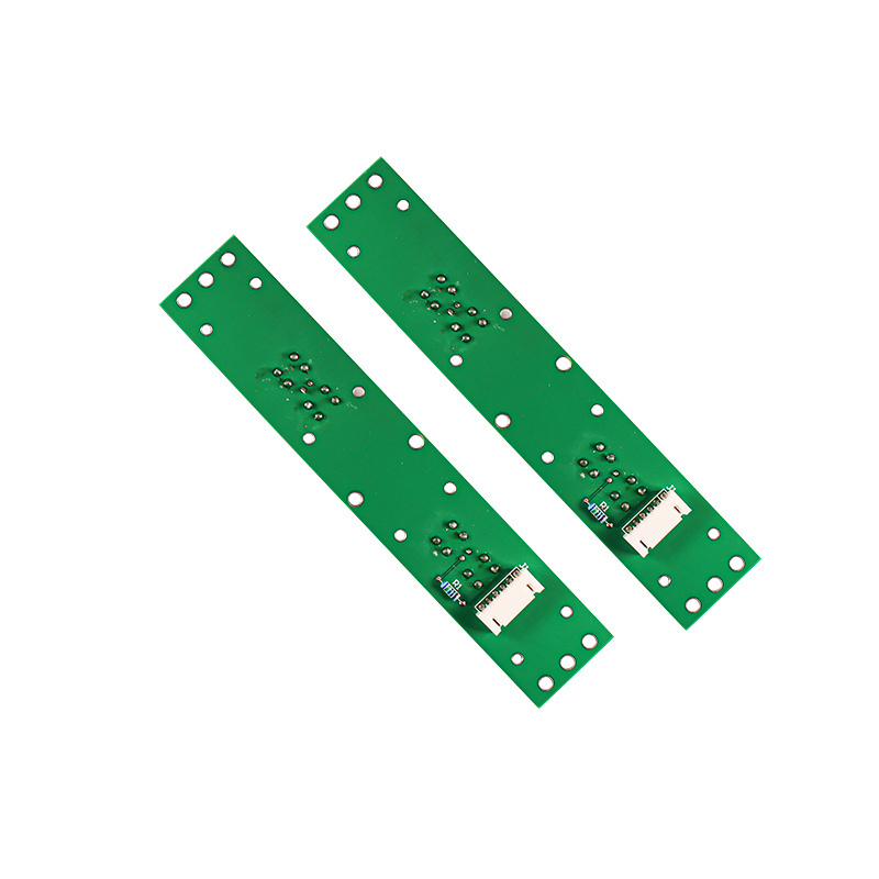
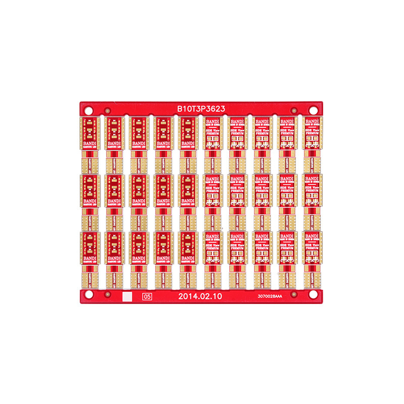
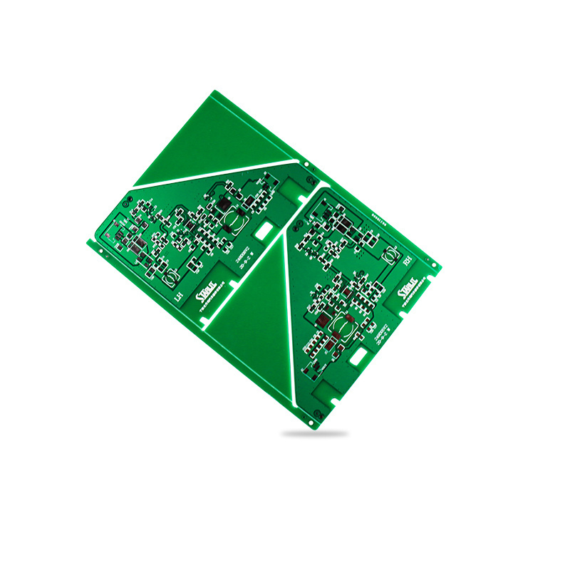
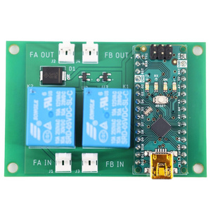
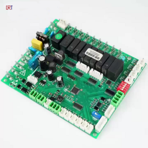
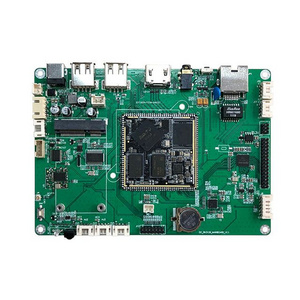
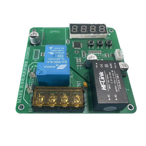
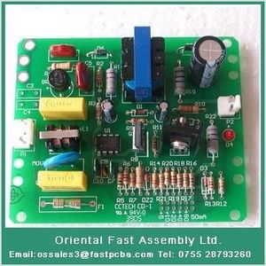
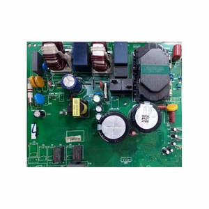
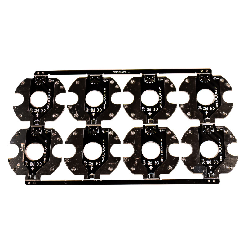
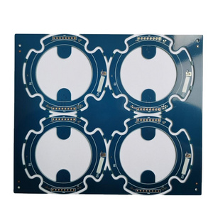
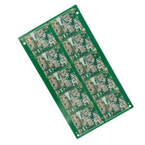
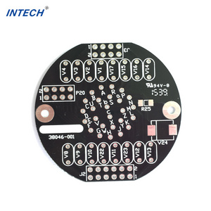
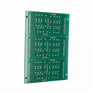
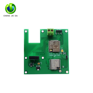
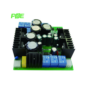
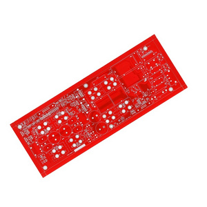
Pcb printing service automotive cob 94v-0 control pcb circuit board kits 4 layer multilayer pcb
|
FR-4 Process capability
|
|
|
|
Item
|
Craft Ability
|
|
|
Surface Finish
|
HASL,Immersion Gold,Gold Plating,OSP,Immersion Tin,etc
|
|
|
Layer
|
1-32 layers
|
|
|
Min.Line Width
|
4mil
|
|
|
Min.Line Space
|
4mil
|
|
|
Min.Space between Pad to Pad
|
3mil
|
|
|
Min.Hole Diameter
|
0.20mm
|
|
|
Min.Bonding Pad Diameter
|
0.20mm
|
|
|
Max.Proportion of Drilling Hole and Board Thickness
|
1:10
|
|
|
Max.Size of Finish Board
|
23inch*35inch
|
|
|
Rang of Finish Board′s Thickness
|
0.21-3.2mm
|
|
|
Min.Thickness of Soldermask
|
10um
|
|
|
Soldermask
|
Green,Yellow,Black,White,Red,transparent photosensitive solder mask,Strippable solder mask
|
|
|
Min.Linewidth of Idents
|
4mil
|
|
|
Min.Height of Idents
|
25mil
|
|
|
Color of Silk-screen
|
White,Yellow,Black
|
|
|
Date File Format
|
Gerber file and Drilling file,Report series,PADS 2000 series,powerpcb series,ODB++
|
|
|
E-testing
|
100%E-Test:High Voltage Testing
|
|
|
Material for PCB
|
High TG Material:High Frequence ROGERS,TEFLON,TADONIC,ARLON(Haloger free Material)
|
|
|
E-testing
|
Impedance Testing,Resisitance Testing,Microsection etc
|
|
|
Special Technological Requirement
|
Blind&Buried Vias and High Thickness Copper
|
|
Recommend Products

Hot Searches
