
- Product Details
- {{item.text}}
Quick Details
-
Board Size:
-
200*300mm, or can be Customized
-
Model Number:
-
JH-MPCB-057
-
Place of Origin:
-
Guangdong, China
-
Brand Name:
-
JinHua
-
Copper Thickness:
-
1OZ
-
Min. Hole Size:
-
0.15mm
-
Min. Line Width:
-
3mil
-
Min. Line Spacing:
-
3mil
-
Surface Finishing:
-
ENIG
-
Product name:
-
quick turn pcb
-
Keywords:
-
custom 4 Layer pcb
-
Special requirements:
-
Blind Vias+Controlled Impedance+BGA
-
MOQ:
-
1 pcs
-
Testing Service:
-
100% AOI Testing
-
Certificate:
-
ISO9001/Iso14001/CE/ROHS/IATF16949
-
Service:
-
OEM multi layer pcb Services Provided
-
Customize:
-
Consumer Electronics
-
Application:
-
Security Equipment
-
PCB Assembly process:
-
DIP SMT PCB Assembly
Quick Details
-
Number of Layers:
-
4-layer
-
Base Material:
-
FR4, CEM, High TG
-
Board Thickness:
-
1.6mm
-
Board Size:
-
200*300mm, or can be Customized
-
Model Number:
-
JH-MPCB-057
-
Place of Origin:
-
Guangdong, China
-
Brand Name:
-
JinHua
-
Copper Thickness:
-
1OZ
-
Min. Hole Size:
-
0.15mm
-
Min. Line Width:
-
3mil
-
Min. Line Spacing:
-
3mil
-
Surface Finishing:
-
ENIG
-
Product name:
-
quick turn pcb
-
Keywords:
-
custom 4 Layer pcb
-
Special requirements:
-
Blind Vias+Controlled Impedance+BGA
-
MOQ:
-
1 pcs
-
Testing Service:
-
100% AOI Testing
-
Certificate:
-
ISO9001/Iso14001/CE/ROHS/IATF16949
-
Service:
-
OEM multi layer pcb Services Provided
-
Customize:
-
Consumer Electronics
-
Application:
-
Security Equipment
-
PCB Assembly process:
-
DIP SMT PCB Assembly
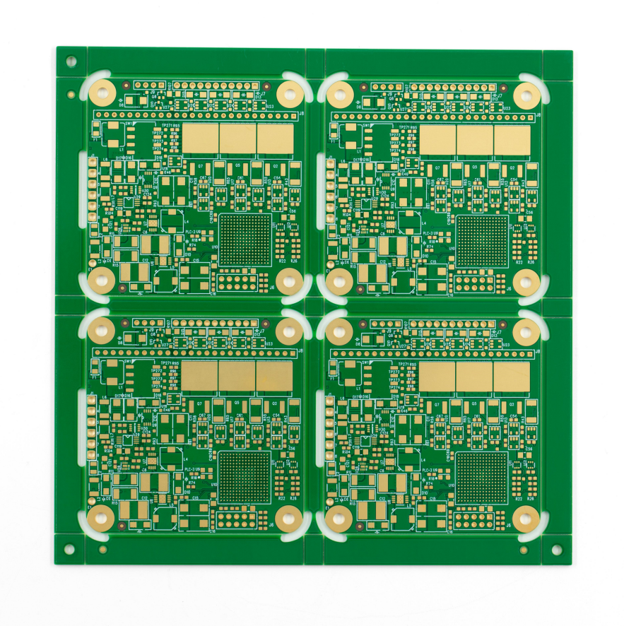
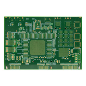
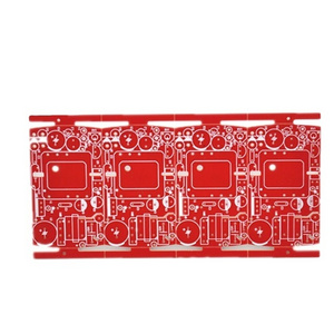
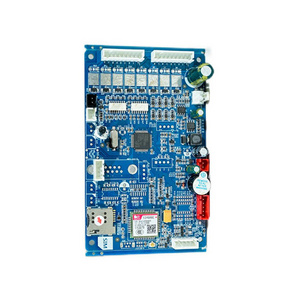
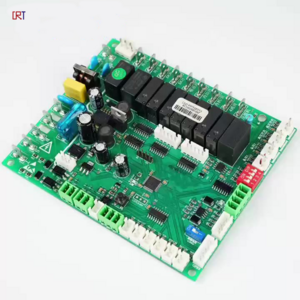
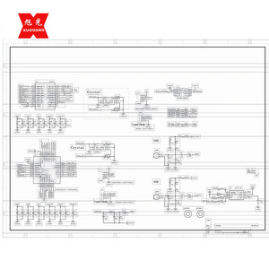
Multilayer PCB is a Printed Circuit Board with more than 2 layers. A Double-Sided PCB has two conductive layers on top and bottom of the PCB substrate. A Multilayer PCB must have a minimum of 3 conductive layers of conductive material or copper layer. All the layers are interconnected with copper plated holes. The layers can be 4, 6, 8…upto 32 layers.


Product Description
| JINHUA PCB Standard Capability | |||
| Item | Process | Manufacturing Capability | Remark |
| 1 | Surface Finishing |
HASL, HASL LF, ENIG, gold fingers plating, OSP, Immersion Ag,
Immersion Sn, Carbon Ink, peelable mask, plug vias with resin |
|
| 2 | Board Thickness | 0.1 MM ~ 8.0 MM | |
| 3 | Layers | 1 ~ 32 L | |
| 4 | Material | Brand: KB, ITEQ, Shengyi, Huazheng,NanYa, CEM, Arlon,Rogers, Teflon, Polymide, panasonic, Aluminum Base, Halogen Free,Peters Soldermask,Kapton high temperature tape, Taiyo Ink | |
| TG: low to high, TG135 to TG180; CTI: 175 to 600 | |||
| 5 | Board Size | Max board size:650 x 1200 MM; Min board size: 3*3 MM | |
| 6 | Inner Layer | (1) ring of line: single sided 4mil | Aspect ratio:10: 1 |
| (2) min trace w/s for 1 OZ:3 mil/2.6mil | Max finished copper thickness:18/18 oz | ||
| (3) hole to line or pad spacing: min 6mil | |||
| 7 | Drilling | (1) min finished hole size: laser 0.1mm mechanical 0.15mm | |
| (2) PTH hole size tolerance: ± 3 mil,NPTH hole size tolerance: ± 2 mil | hole position registration tolerance: ± 2 mil | ||
| (3) min slot size:0.55 mm | |||
| 8 | Outer Layer | (1) 1oz: 3/3 mil, 2oz:5/5 mil | Max finished copper thickness:18/18 oz |
| 9 | Plating | (1) hole wall copper thickness 1-10 mil | |
| (2) 10:1 | |||
| 10 | Soldermask | (1) min soldermaks bridge 4mil | min PAD 20 mil |
| 11 | Silkscreen | Color:white, black, yellow, red...etc. | Serial number, Barcode, QR code |
| 12 | Profiling | (1) Tolerance of outline: ± 0.1mm | |
| (2) V-CUT Angle: 30 degree & 45 degree | min V-Cut width 75 MM | ||
|
(3) Depth:Board thickness≥1.2 mm Remain thicknss: 1/3;
Board thickness≤1.2 mm, remain thickness 20 mil (0.5 mm) |
min distance V-Cut to copper 0.4 MM | ||
| (4) Bevelling angle/depth: 20°/1.8 mm;30° /1.0 mm;45°/0.5 mm;tolerance:± 5°/± 0.2 mm | |||
| 13 | Bow and Twist | 1L≤1.0% 2L≤0.75% Multi layers≤0.75% | |
| 14 | Monthly Capcity | 120,000 M2 | |
| Layer | Quick Turn/Usual Time | Mass Production |
| 2L | 24 hours/4-5 days | 8-10 days |
| 4L | 48 hours/6-7 days | 10-12 days |
| 6L | 72 hours/7-8 days | 12-14 days |
| 8L | 72 hours/8-10 days | 16-18 days |
| 10L | 96 hours/12-14 days | 18-20 days |
Hot Searches
