Explore More Products
- Product Details
- {{item.text}}
Quick Details
-
Supplier Type:
-
Customized
-
Layers:
-
1-58 layers
-
Certificate:
-
ISO TS16949
-
Surface treatment:
-
HASL, HASL LF, etc.
-
Solder mask:
-
Double -sided green LPI/ customized
-
File needed:
-
Gerber.BOM LIST
-
Material:
-
FR-4 / High TG FR-4 / Halogen Free.etc
-
Service:
-
Offer PCBA design
-
MOQ:
-
1 PCS
-
Layer:
-
1-58 Layers
-
Color:
-
BLACK/ WHITE/GREEN
Quick Details
-
Model Number:
-
PCBA-20
-
Place of Origin:
-
Guangdong, China
-
Brand Name:
-
XZH
-
Supplier Type:
-
Customized
-
Layers:
-
1-58 layers
-
Certificate:
-
ISO TS16949
-
Surface treatment:
-
HASL, HASL LF, etc.
-
Solder mask:
-
Double -sided green LPI/ customized
-
File needed:
-
Gerber.BOM LIST
-
Material:
-
FR-4 / High TG FR-4 / Halogen Free.etc
-
Service:
-
Offer PCBA design
-
MOQ:
-
1 PCS
-
Layer:
-
1-58 Layers
-
Color:
-
BLACK/ WHITE/GREEN
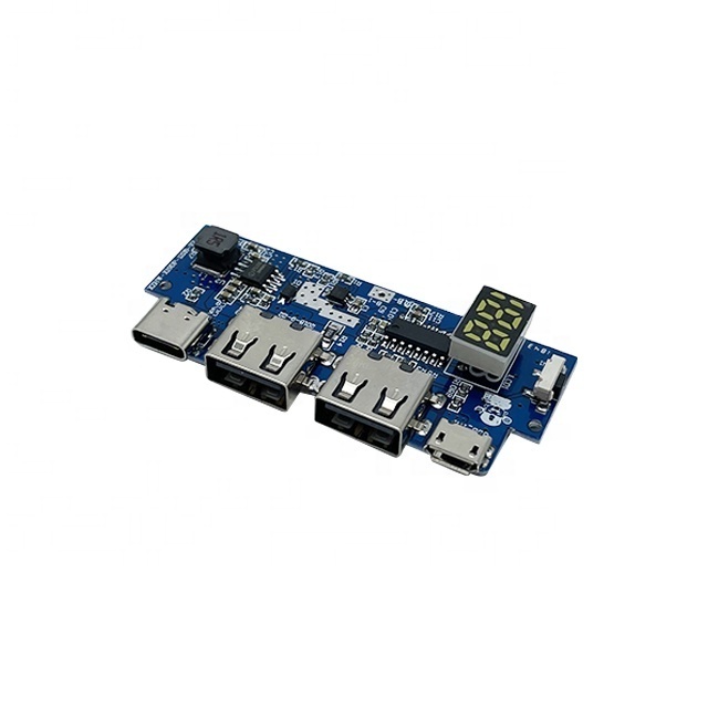
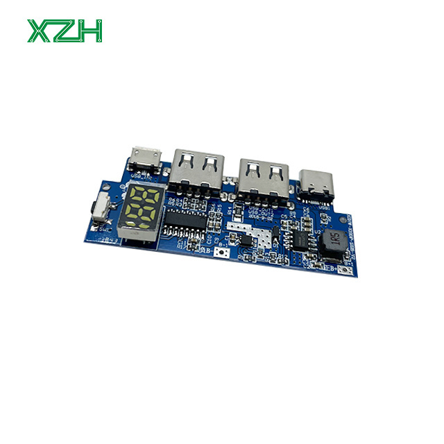
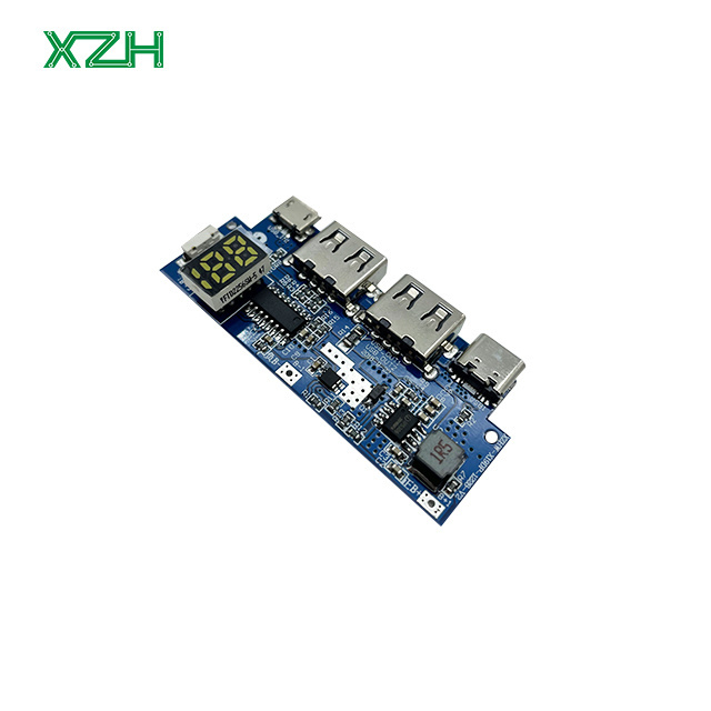
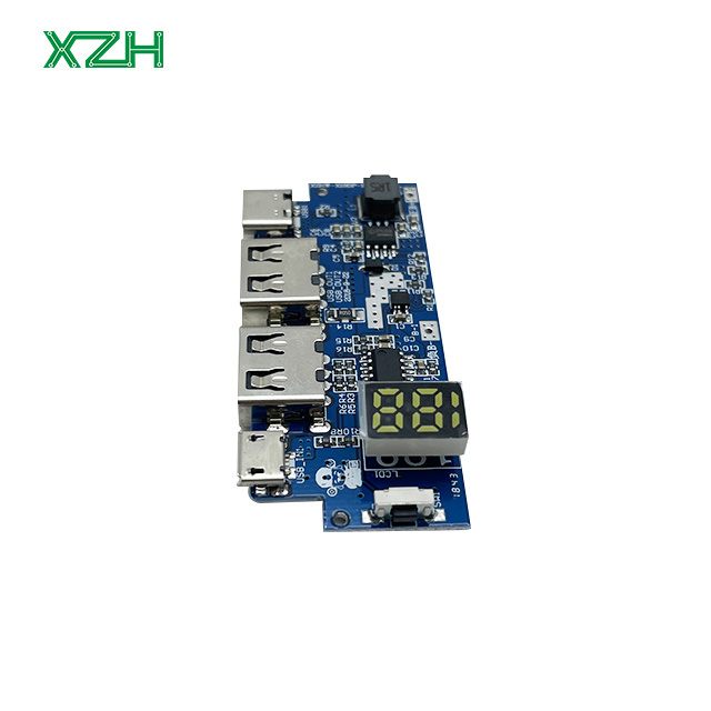
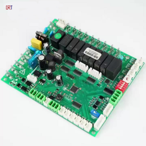
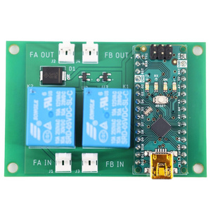
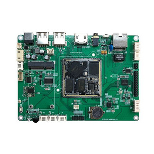
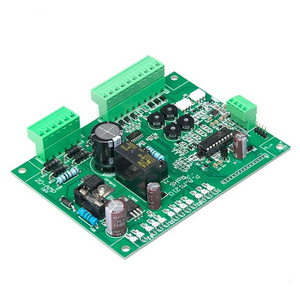
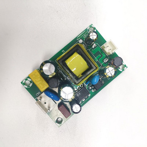
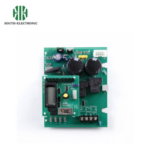
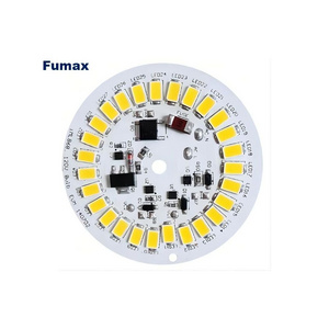
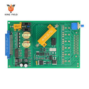
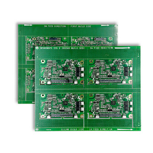
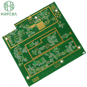
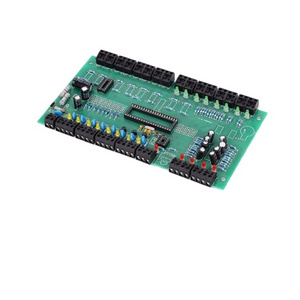
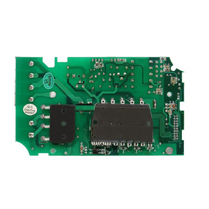
Oem Customized Power Bank Board Pcb Pcba
XZH: Your One-Stop ODM/OEM Solution Provider
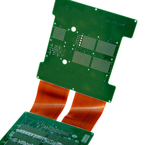
Product Introduction
|
Layers
|
1-58 layers
|
|
Board material
|
FR-4 / High TG FR-4 / Halogen Free material/Rogers/Arlon/Taconic/Teflon
|
|
Surface treatment
|
HASL, HASL lead free, Immersion Gold, Immersion Tin, r, Hard gold, Flash gold, OSP…
|
|
Silk screen colour
|
White / Black / Yellow
|
|
Solder mask colour
|
Green / Blue / Red / Black / Yellow / White
|
Production Capabiity
|
Item
|
Capability
|
|
Base Material
|
FE-4/High TG FR-4/Lead Free Materials (ROHS Compliant)/Halogen Free Material/CEM-3/
CEM-1/PTFE/GOGERS/ARLON/TACONIC
|
|
Layers
|
1-28
|
|
Finised Inner/
Outter Copper Thickness
|
1-6OZ
|
|
Finised Board Thickness
|
0.2-7.0mm
|
|
|
Tolerance: Board Thickness ≤1.0mm: +/-0.1mm
1<Board Thickness≤2.0mm: +/-10%
Board Thickness>2.0mm: +/-8%
|
|
Max Panel SIze
|
≤2 sides PCB: 600*1500mm; Multilayer PCB:500*1200mm
|
|
Min Cinductor Line Wideth/Spacing
|
Inner Layers: ≥ 3/3mil
Outer Layers: 3.5/3.5mil
|
|
Min Hole Size
|
Mechanical Hold: 0.15mm; Laser Hole: 0.1mm; Drilling Precision: First drikking: 1mil, Second drilling: 4mil
|
|
Warpage
|
Board Thickness ≤0.79mm: β≤1.0%
0.80≤Board Thickness≤2.4mm: β≤0.7%
Board Thickness ≤2.5mm: β≤0.5%
|
|
Controlled Impedance
|
+/-5%
|
|
Aspect Ratio
|
15:01
|
|
Min Welding Ring
|
4mil
|
|
Min Solder Mask Bridge
|
≥0.08
|
|
Plugging Vias Capbility
|
0.2-0.8mm
|
|
Hole Tolerance
|
PTH: +/-3mil; NPTH: +/-2mil
|
|
Outline Profile
|
Rout/V-cut/Bridge/Stamp Hole
|
|
Surface Treatment
|
OSP:0.5-0.5um HASL:2-40um
Lead free Hasl:2-40um ENIG:Au 1-10U"
ENEPIG:PB 2-5U""/Au 1-8U'' Immersion Tin:0.8-1.2um
Immersion silver:0.1-1.2um Peelable Blue Mask
Carbon Ink Gold plating:Au 1-150U'
|
|
E-testing Pass Percent
|
97% Pass For The First Time,+/-2%(tolerance)
FQC-Physical Lab:Reliability Tests
|
|
Certificate
|
ROHS, ISO9001:2015, IS013484:2016, IPC3 Staandard
|


For PCB (Printed Circuit Board) and PCBA (Printed Circuit Board Assembly) logo customization, the logo can be applied to the following areas:
1. PCB Surface: Logos can be printed on the surface of the PCB, typically in an edge area or a designated non-functional zone.
2. PCBA Assembled Components: If there are visible plastic or other non-conductive material parts on the PCBA, logos can also be printed on these components.
3. Packaging Materials: The exterior or interior packaging for PCBs or PCBAs can feature logos, including packaging boxes, plastic bags, or anti-static bags.
The methods for imprinting logos generally include:
1. Screen Printing: Suitable for PCB surfaces and packaging materials, allowing for single or multi-color logo imprints.
2. Inkjet Printing: Enables high-resolution color printing on PCBs or packaging materials.
3. Laser Marking: Ideal for creating permanent logos on non-conductive parts of PCBs or on metal surfaces.
4. Hot Stamping: Adds a tactile finish to packaging materials with logo imprints.
5. Labeling: Applying labels or stickers with logos onto the PCB or PCBA.
Custom packaging options may include:
1. Standard Packaging: Using standard anti-static bags or plastic bags with custom labels on the exterior.
2. Custom Packaging Boxes: Designing and manufacturing packaging boxes with logos based on customer requirements.
3. Eco-friendly Packaging: Packaging made from recyclable or biodegradable materials to reflect environmental sustainability.
4. Shockproof Packaging: Custom shockproof packaging for fragile PCBs or PCBAs that require additional protection.
5. Gift Box Packaging: Custom gift box packaging designed for high-end products or special occasions.
In addition to our comprehensive customization services, we also offer collaborative procurement assistance for a wide range of products. Our goal is to streamline your process and save you valuable time.
Click the CHAT NOW button below to contact our salespeople.
Hot Searches
