Explore More Products
- Product Details
- {{item.text}}
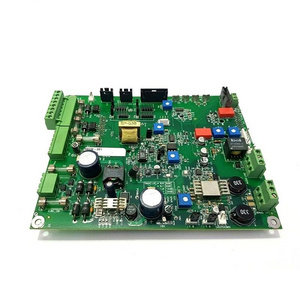
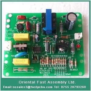
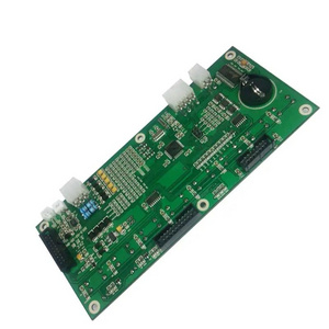
Quick Details
-
Supplier Type:
-
Custom
-
Copper Thickness:
-
1 oz~30 oz
-
Product name:
-
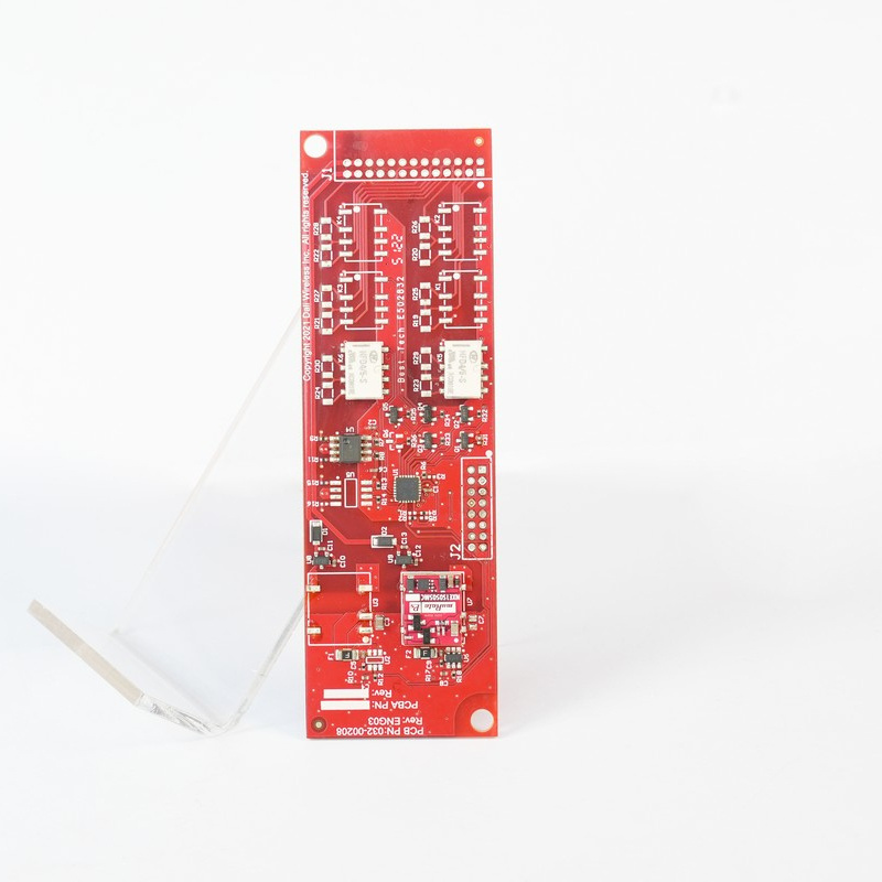
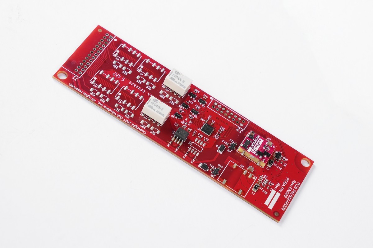
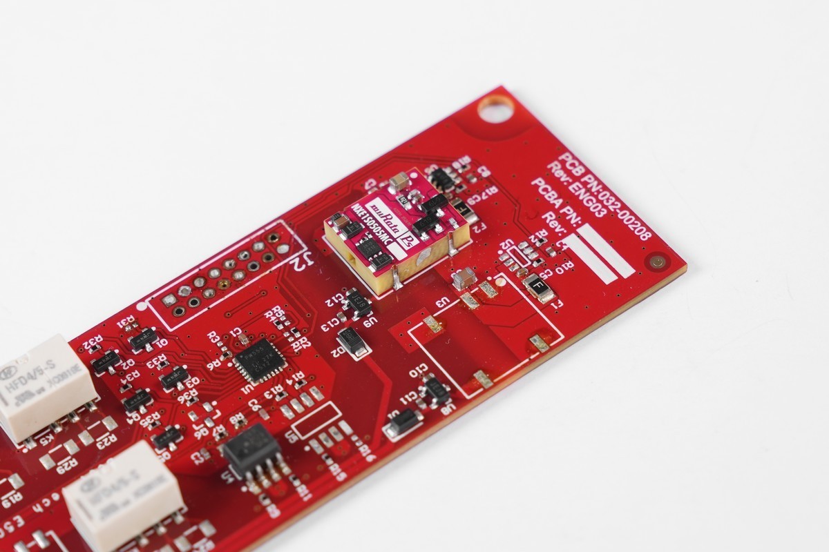
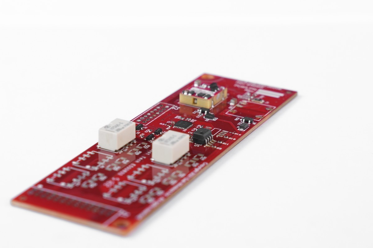
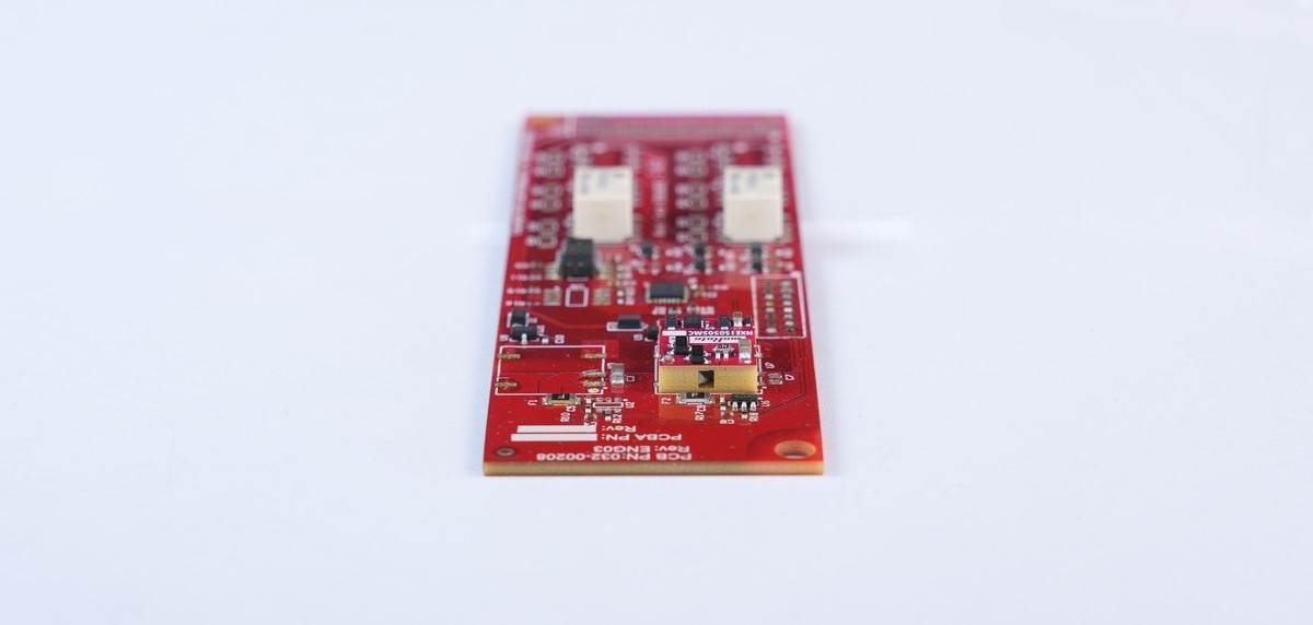
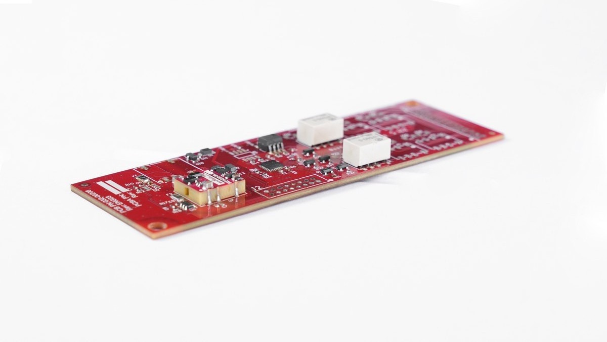
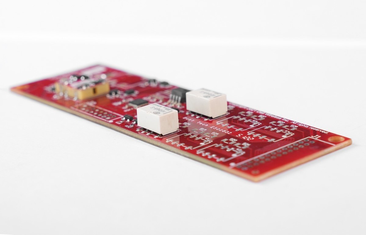
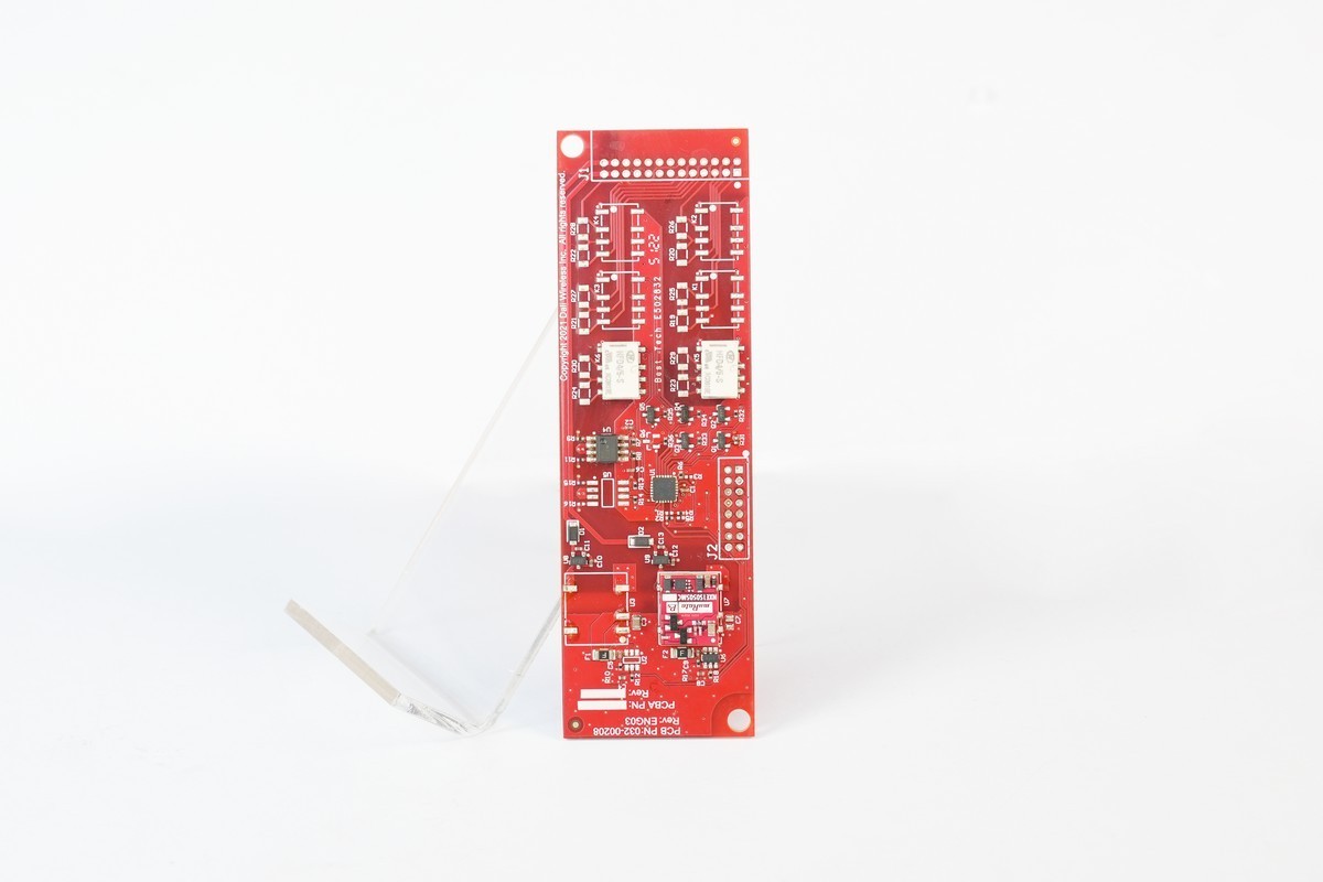
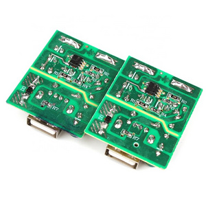
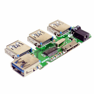
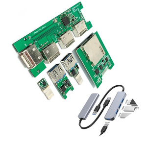
Multi-Layer PCBA
-
Certificate:
-
IATF16949/UL
-
Base Material:
-
FR4
-
Assembly Type:
-
SMD SMT DIP Components Assembly
-
Testing Type:
-
3D AOI, X-RAY, ICT Functional testing
-
Printing accuracy:
-
0.022mm
-
Mounting speed:
-
0.0378s/point
-
High speed placement machine:
-
YSM20R
-
Soldermask Color:
-
Red
-
Silkscreen Color:
-
White
Quick Details
-
Model Number:
-
BPM15025
-
Place of Origin:
-
Guangdong, China
-
Brand Name:
-
Danyu
-
Supplier Type:
-
Custom
-
Copper Thickness:
-
1 oz~30 oz
-
Product name:
-
Multi-Layer PCBA
-
Certificate:
-
IATF16949/UL
-
Base Material:
-
FR4
-
Assembly Type:
-
SMD SMT DIP Components Assembly
-
Testing Type:
-
3D AOI, X-RAY, ICT Functional testing
-
Printing accuracy:
-
0.022mm
-
Mounting speed:
-
0.0378s/point
-
High speed placement machine:
-
YSM20R
-
Soldermask Color:
-
Red
-
Silkscreen Color:
-
White
Product Description
About Us
Customer Visit
Manufacturing Capability
|
Prototype
|
Components size ≥0402, no DIP
|
1 W
|
|
|
Components size ≥0402, with DIP
|
1-2 W
|
|
|
Components size ≤0201,no DIP
|
1-2 W
|
|
|
Components size ≤0201, with DIP
|
1.5~2 W
|
|
Production
|
Components size ≥0402, no DIP
|
1.5~2 W
|
|
|
Components size ≥0402,with DIP
|
1.5~2.5 W
|
|
|
Components size ≤0201,no DIP
|
2~3W
|
|
|
Components size ≤0201,with DIP
|
2.5~3.5 W
|
Notes: Customers provided components. If BOM purchased by us, 1 week will be added for most of cases. For components without stock, or with longer lead time, L/T will be negotiated with customers.
Advantage
Package & Shipment
Customer Evaluation
FAQ
1.What size board can your AOl scan?AOl effective scanning stroke: length: 25-480mm interval range, width: 25-330mm intervalrange;
2.What size board can your X-RAY scan?
The maximum payload size of X-RAY is 510*420mm, and the effective scanning stroke is435*385mm
3.What is the size and spacing of the solder joints you can work with?
The min solder PAD we can solder is 0.15mm, and the distance between PAD is 0.2mm
4.What is the minimum size of material you can paste?
The min components we can solder is with the footprint 1005
5.How thick stencil you can make?
We can make 0.08mm,0.10mm,0.12mm solder stencil
6.What is the tolerance of the placements of the surface mountedcomponents? Regarding the tolerance for the placements of the SMT components, according to thestandard of IPC 6012 class 2, the placement is not allowed to exceed 1/2 of the PAD on thePCB. And if customers required us to follow the production with IPC 6012 class 3, then theplacement is not allowed to exceed 1/3 of the PAD on the PCB.
7.What is the minimum width of the pad you can weld wire to?
If it is for wires assembly, the PAD size need to be 20% bigger than the wires size. lf it is acommon components, the PAD size need to be 10% bigger than the wires components, ifthe PAD size is equal to the components size, that's also workable for us to solder, but itwill be better for soldering if 10% bigger.
Hot Searches
